- Department of Electrical Engineering and Information Systems, The University of Tokyo, Tokyo, Japan
Breakdown is one of main failure mechanisms that limit write endurance of ferroelectric devices using hafnium oxide-based ferroelectric materials. In this study, we investigate the gate current and breakdown characteristics of Hf0.5Zr0.5O2/Si ferroelectric field-effect transistors (FeFETs) by using carrier separation measurements to analyze electron and hole leakage currents during time-dependent dielectric breakdown (TDDB) tests. Rapidly increasing substrate hole currents and stress-induced leakage current (SILC)-like electron currents can be observed before the breakdown of the ferroelectric gate insulator of FeFETs. This apparent degradation under voltage stress is recovered and the time-to-breakdown is significantly improved by interrupting the TDDB test with gate voltage pulses with the opposite polarity, suggesting that defect redistribution, rather than defect generation, is responsible for the trigger of hard breakdown.
1 Introduction
HfO2-based ferroelectric thin films have been actively employed in recent electron device research thanks to their CMOS compatibility, established know-how on the fabrication process, and high scalability of thickness to 10 nm or lower (Böscke et al., 2011a; Müller et al., 2012; Park et al., 2015; Kim et al., 2018; Migita et al., 2018; Tan et al., 2021; Toprasertpong et al., 2022a; Schroeder et al., 2022). Ferroelectric field-effect transistors (FeFETs) with HfO2-based ferroelectric thin films as gate insulators have received considerable attention, not only because of the maturity of the HfO2 deposition technology in the advanced transistor process, but also because of their low energy consumption, high speed, and satisfactory retention during their operation. HfO2-based FeFETs have been investigated as promising devices for low-power non-volatile memory (Böscke et al., 2011b; Trentzsch et al., 2016; Dünkel et al., 2017; Florent et al., 2018a; Müller et al., 2021) and non-von Neumann computing applications (Jerry et al., 2018; Dutta et al., 2020; Matsui et al., 2021; Toprasertpong et al., 2022b; Luo et al., 2022).
Despite their excellent properties, one of the most crucial issues to be dealt with towards the practical use of HfO2-based FeFETs is the write endurance. There are two major mechanisms that have been reported to determine the write endurance of FeFETs: the memory window narrowing and gate dielectric breakdown. The memory window narrowing refers to a phenomenon where a separation of the threshold voltages of the two states (high and low threshold voltage states) becomes gradually smaller and eventually becomes zero after certain operating cycles. The polarization states are no longer able to be read out through threshold voltages and FeFETs lose a capability as memory devices. On the other hand, gate dielectric breakdown refers to a situation where the gate insulator experiences hard breakdown under a certain amount of electrical stress. Hard breakdown makes gate insulators conductive, electrically connects the gate and channel, and causes FeFETs to lose their function as field-effect transistors.
Memory window narrowing and gate dielectric breakdown originate from different physics and occur almost independently; therefore, the write endurance of FeFETs, i.e., a number of write operations before failure, is determined by the mechanism that leads to earlier failure. The dominant mechanism depends on the device property and the operation scheme of each specific device and application. Write endurance of state-of-the-art FeFETs is typically dominated by the memory window narrowing (Böscke et al., 2011b; Trentzsch et al., 2016; Yurchuk et al., 2016; Dünkel et al., 2017; Florent et al., 2018a; Gong et al., 2018) because of the presence of large density of trapped charges in the vicinity of the interfacial layer (IL) between HfO2 and Si (Toprasertpong et al., 2019; Toprasertpong et al., 2020a), while there are only a few reports showing that endurance of FeFETs is limited by gate dielectric breakdown (Ni et al., 2018; Peng et al., 2021). That is, the FeFET operation so far usually reaches failure because of memory window narrowing before gate dielectric breakdown occurs; thus, there is still a poor understanding of the gate dielectric breakdown mechanism in HfO2-based FeFETs. On the other hand, a lot of effort has been put on the material and device-structure engineering such that there have already been some reports in recent years demonstrating FeFET memory devices with remarkably suppressed memory window narrowing (Sharma et al., 2020; Yan et al., 2020; Tan et al., 2021; Liao et al., 2022). In such devices with suppressed memory window narrowing, gate dielectric breakdown may become a dominant mechanism that limits write endurance and play a crucial role in device reliability. Furthermore, there are some applications of FeFETs using new-concept computing that are insensitive to memory window narrowing, such as reservoir computing (Nako et al., 2022). In such applications, gate dielectric breakdown will be a dominant endurance-limiting mechanism. Therefore, gaining an understanding of the mechanism of gate dielectric breakdown is important to improve the overall write endurance characteristics of HfO2-based FeFETs.
In this study, we investigate the breakdown characteristics and the stress-induced degradation behavior as well as the underlying physical mechanism in Hf0.5Zr0.5O2 (HZO)/IL/Si FeFETs. The carrier separation measurement and interrupted stress for time-dependent dielectric breakdown (TDDB) evaluation are employed to analyze the physical mechanism underlying gate dielectric breakdown.
2 Sample preparation
The process flow is shown in Figure 1A. We fabricated n-channel non-ferroelectric FETs (called here as non-ferro-FET) with a paraelectric HfO2 gate insulator and FeFETs with a ferroelectric HZO gate insulator on p-type Si substrates with a moderate doping concentration of 4×1015 cm−3. After the source and drain (S/D) regions were doped by phosphorus ion implantation and annealed to activate dopants, the Si substrates were cleaned by hydrochloric-peroxide mixture (HPM)-last cleaning process to grow a high-quality SiO2 IL (Toprasertpong et al., 2020b). For FeFETs, 10-nm-thick ferroelectric HZO was deposited by atomic layer deposition (ALD) using at using tetrakis (ethylmethylamino)hafnium (TEMAH), tetrakis (ethylmethylamino)zirconium (TEMAZ), and H2O at 300°C. For non-ferro-FETs, 10-nm-thick HfO2 was deposited in a similar way but without TEMAZ. TiN was deposited as gate metal by sputtering and silicon-doped aluminum was deposited as S/D contacts by thermal evaporation. Samples were annealed at 400°C for 30 s in a N2 atmosphere to crystalized the ferroelectric phase in FeFETs. The non-ferro-FETs were also annealed at the same condition. Except the ALD step, both samples were processed simultaneously in the same chamber to ensure the same device condition. Figures 1B, C show transmission electron microscopic (TEM) images of the gate stacks of a non-ferro-FET and a FeFET, respectively, indicating that HZO was crystallized whereas HfO2 remained amorphous. The IL thickness was similar in the both samples.
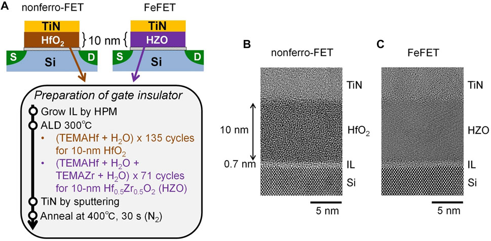
FIGURE 1. (A) Fabrication process flow. TEM images of (B) HfO2 non-ferro-FET and (C) HZO FeFET. HZO was crystallized whereas HfO2 remained amorphous.
3 Results and discussion
3.1 Band diagram and breakdown position
Before we discuss the experimental results of the leakage and breakdown behaviors, we examine the band diagram of the HZO (10 nm)/IL (0.7 nm)/Si gate stack and the possible gate leakage path. Figure 2A depicts an example of an ideal band diagram of the HZO/IL/Si gate stack at 3 V when HZO has ferroelectric polarization of 10 μC/cm2. Due to high ferroelectric polarization, most literature considers a band diagram with a strong electric field across the IL, which significantly pulls down the band position HZO, as shown in Figure 2A (Müller et al., 2016; Yurchuk et al., 2016; Gong et al., 2018; Mulaosmanovic et al., 2021; Peng et al., 2021). In such a case, the breakdown of the IL is supposed to determine the gate dielectric breakdown of FeFETs. However, it has been reported that a large density of trapped charges near the HZO/IL interface electrically screens the polarization and suppresses the electric field across the IL (Toprasertpong et al., 2019; 2022c). Figure 2B depicts the band diagram with ferroelectric polarization of 10 μC/cm2 and 90% (Ichihara et al., 2020) of induced electrons are trapped at the HZO/IL interface. It can be seen that the band of HZO is not at such a low energy position. This fact indicates that electrons have to tunnel through a thick HZO layer and thus the breakdown of HZO is necessary to describe the gate breakdown failure of FeFETs.
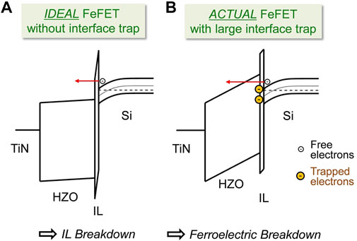
FIGURE 2. Schematic band diagram of HZO/IL/Si gate stack (A) when there is no interface charge trapping and (B) when there is a large amount of interface charge trapping, where 90% of induced electrons are trapped. Here, the Si band was scaled in the depth direction by 1:100 ratio to make the band bending clear.
3.2 Device characteristics
The I-Vg characteristics of the non-ferro-FET and FeFET are shown in Figures 3A, B, respectively, for gate current Ig, drain current Id, source current Is, and substrate current Isub. A gate length L is 10 μm and a gate width W is 100 μm. As expected, the non-ferro-FET exhibits the Id-Vg characteristics with clockwise hysteresis, which is a feature of electron trapping during Vg scans. On the other hand, the FeFET exhibits counterclockwise hysteresis, which is a feature of ferroelectricity, with a memory window of approximately 1.8 V. Comparison of the I-Vg characteristics of the non-ferro-FET and FeFET indicates interesting features on Ig and Isub. Gate current Ig in the HZO FeFET is much larger by several orders of magnitude than in non-ferro-FETs having HfO2 with a similar physical thickness. This can be understood from the fact that the poly-crystallinity and a lot of defects such as oxygen vacancies in HZO can promote the gate leakage current, as shown in Figure 3C. It is also found that the substrate current Isub in the FeFET rapidly increases by four orders of magnitude in a narrow range of Vg = 3.6 V–4.0 V during the forward Vg scan, which is in the same range that Ig also increases rapidly by two orders of magnitude. This finding suggests that a study of the behavior of Isub would be helpful in understanding the behavior of the gate leakage and gate dielectric degradation. The non-ferro-FET in Figure 3A does not exhibit this Isub behavior.

FIGURE 3. Characteristics of Ig, Id, Is, and Isub for (A) HfO2 non-ferro-FET and (B) HZO FeFET with L/W = 10/100 μm. Ig of a HZO FeFET is around 103 times higher than that of a HfO2 non-ferro-FET. Steeply increasing substrate current Isub can be found in FeFETs. (C) Leakage current path in ferroelectric HZO gate insulator.
3.3 Carrier separation measurements
Carrier separation measurements (Eitan et al., 1983; Weinberg et al., 1985) were carried out to analyze the behavior of gate leakage and gate dielectric degradation. The electrical measurement tool (Keysight B1500A with high-resolution source/monitor unit modules) was connected with FETs in a way shown in Figure 4A, where Vd = Vs = Vsub = 0. The current detected at the S/D terminal corresponds to the electron component of gate current, denoted by Ie, while the current detected at the substrate corresponds to the hole component, denoted by Ih. When Vg is larger than the threshold voltage, Ie corresponds to the tunneling current of inversion electrons from the Si substrate to the gate, whereas Ih corresponds to the sum of the tunneling current of valance-band electrons in the Si substrate to the gate (Weinberg et al., 1985; Schuegraf et al., 1994b; Shanware et al., 1999) and the tunneling back current of holes from the gate to the Si substrate (Schuegraf et al., 1994a; Schuegraf et al., 1994b; Kobayashi et al., 1995), as illustrated in Figure 4B.
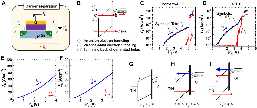
FIGURE 4. (A) Schematic of carrier separation measurement for analyzing gate current. (B) Current components in gate current. Inversion electron tunneling flows through S/D, while tunneling of valence-band electrons and generated holes appears as substrate current. Electron-component (blue lines), hole-component (red lines), and total (circle symbols) gate currents of (C) non-ferro-FET and (D) FeFET when Vg was scanned from 0 V until the breakdown point. The electron component dominates the gate current while the hole component rapidly increases near the breakdown voltage. Gate currents after breakdown for (E) non-ferro-FET and (F) FeFET, showing ohmic characteristics. Band diagrams and expected gate current components at (G) low Vg, (H) Vg < VBD, and (I) Vg > VBD.
The results of the carrier separation measurements are shown in Figures 4C, D for the HfO2 non-ferro-FET and HZO FeFET, respectively. In these measurements, Vg of pristine samples was scanned from 0 V to the positive voltage where breakdown occurs. It can be seen that tunneling of inversion electrons is the main contribution of Ig for both the non-ferro-FETs and FeFET. Ih is found to be under detection limit in a low Vg regime, but it rapidly increases at Vg close to the breakdown voltage. The breakdown voltage VBD of the non-ferro-FET is approximately 5.2 V, whereas the FeFET reaches hard breakdown much earlier at approximately VBD = 4.1 V. Earlier breakdown is contributed to more defects in HZO than those in HfO2, in agreement with larger gate current shown in Figures 3A, B. Hard breakdown of the non-ferro-FET occurs at comparatively low Ih, whereas Ih of HZO FeFET keeps noisy until very high level of Ih. After breakdown, the electrical properties of the gate insulators of both the devices become ohmic and dominated by electron current, as shown in Figures 4E, F.
The band alignments are shown in Figures 4G–I. At small Vg, it is clear from the band alignment that electrons in the conduction band of Si can easily tunnel to the gate. At Vg in the mid-range, both electrons in the valence band and holes generated at the gate can tunnel more easily, resulting in increasing Ih. At large Vg, an electric field across HZO is so large that hole tunneling back can reach the valence band of HZO, resulting in large Ih. Increasing hole tunneling back consequently causes breakdown in the gate insulator, as the hole tunneling back is known to be the main cause of damage in the gate insulator (Schuegraf et al., 1994a; Schuegraf et al., 1994b; Takayanagi et al., 2001).
Results of repeated measurements of Ie and Ih in a Vg scan range of −2 V to 4 V are shown in Figure 5. It is interesting that rapidly increasing Ih and Ie at Vg > 3.5 V in the FeFET, together with noisy signals before breakdown, are recovered during the Vg backward scan, resulting in repeatable Ih-Vg and Ie-Vg characteristics. These results imply that, although rapidly increasing Ih is an indication that breakdown is going to be triggered, the permanent degradation still does not occur yet in this condition and occurs when Ih increases in a step-wise manner, which can be observed in Figure 4D at Vg = 4.1 V.
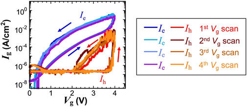
FIGURE 5. Repeatedly measured electron and hole components of Ig in the FeFET. Repeatable current implies that it is not a behavior of permanent trap generation.
The analysis above suggests that Ih is a convenient indicator for determining appropriate operating range of Vg. Figure 6 shows the I-Vg characteristics of the FeFET when Vg was kept below 3.5 V. In this Vg range, the ferroelectric hysteresis can still be achieved with a satisfactory memory window of 1.7 V while Ih is suppressed to under the detection limit. Note that Isub at negative Vg is due to gate-induced drain leakage (GIDL), which is unrelated to gate leakage currents. Although Ih does not necessarily imply to device degradation as discussed in Figure 5, hole tunneling back is flowing and leads to a higher probability that breakdown is triggered; therefore, the operating condition with high Ih should be avoided. The reliability of FeFETs operating in this way is notably improved and we cannot observe breakdown under electrical stress for a practically long time (>105 s).
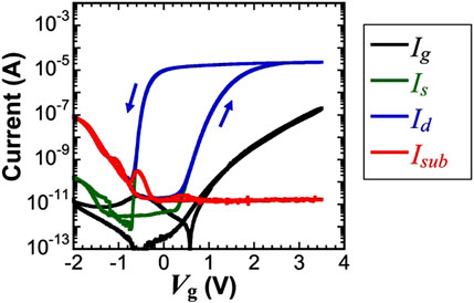
FIGURE 6. Characteristics of Ig, Id, Is, and Isub for HZO FeFET with L/W = 10/100 μm when the Vg ranged is limited below 3.5 V. No substrate current Isub is observed at positive Vg.
3.4 Time-dependent dielectric breakdown: Constant voltage stress and interrupted test
TDDB tests with a carrier separation setup were carried out to gain more insights into the breakdown behavior of FeFETs. Ie(t) and Ih(t) under constant voltage stress (CVS) as a function of stress time t are shown in Figures 7A, B for non-ferro-FETs and FeFETs, respectively. Both Ie(t) and Ih(t) of the FeFET increase with time, which is in the opposite direction of Ie(t) of non-ferro-FETs in the early stage. Note that Ih of non-ferro-FETs is so low that cannot be measured until breakdown, indicating that there is less hole tunneling back in non-ferro-FETs. We call the behavior of FeFETs having Ie(t) increasing with time as a SILC-like behavior, as stress-induced leakage current (SILC) refers to a phenomenon that a leakage current increases with electrical stress. This SILC-like behavior of Ie(t) of FeFETs can be fitted with a power-law function to be
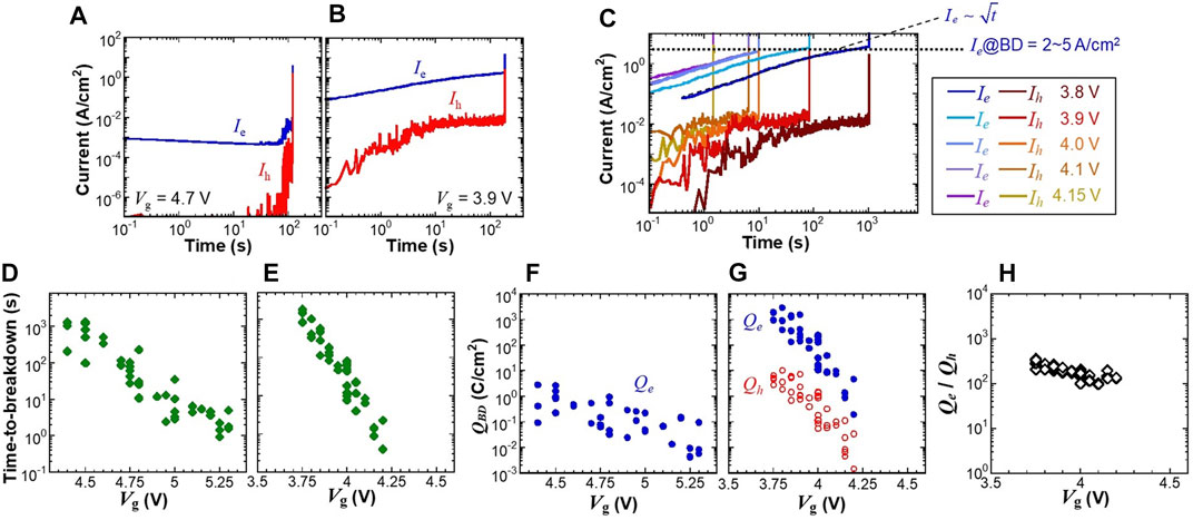
FIGURE 7. TDDB results with carrier separation for (A) HfO2 non-ferro-FET at Vg = 4.7 V and (B) HZO FeFET at Vg = 3.9 V with L/W = 100/100 μm. A SILC-like behavior, with current increasing with stress time, can be observed in FeFETs. (C) TDDB of FeFET at different stress voltage Vg. Electron current increases with time by approximately
Time-to-breakdown tBD under CVS are summarized in Figures 7D, E for non-ferro-FETs and FeFETs, respectively. Not only the breakdown at lower Vg than non-ferro-FETs but also tBD more sensitive to Vg can be observed for FeFETs, with tBD of approximately 103 s at Vg = 3.75 V reduced to approximately 10–1 s at Vg = 4.2 V. The results of charge-to-breakdown QBD for electrons Qe =
We have observed from Figure 7B that gate leakage increases with stress time, as similar to a SILC-like behavior. Here, we investigate the device behavior during the increase of gate leakage current. Figures 8A, C show the I-Vg characteristics before and after a CVS at 4 V for 10 s shown in Figure 8B. Although Ie(t) and Ih(t) increase by approximately 100 times during the 10-s CVS test, it is found that an only small change of the I-Vg characteristics can be observed after stress. This implies that increases of Ie(t) and Ih(t) in FeFETs are not similar to typical SILC, where increasing current cannot be easily recovered: Increasing currents in FeFETs can be recovered after releasing the stress.

FIGURE 8. (A) I-Vg characteristics of FeFET before CVS. (B) Electron and hole components of gate leakage current under CVS at Vg = 4 V for 10 s (C) I-Vg characteristics of FeFET after CVS. Although gate current increases during CVS, it has a negligible effect on I-Vg characteristics.
This peculiar behavior of the gate leakage current is further investigated by applying interrupt pulses during TDDB tests. Figure 9A displays a voltage waveform when TDDB tests stressed at Vg = 4 V were interrupted by Vg = 0 V for 1 s every stress time of ts. Figures 9B, C show Ie(t) and Ih(t) for each stress cycle when ts = 10 s (cycles of 4 V for 10 s and 0 V for 1 s). Ie(t) and Ih(t) increase cycle by cycle regardless of interrupts by 0 V, implying that electrical stress keeps accumulated. Figure 9D summarizes the time-to-breakdown tBD (excluding interrupt time at 0 V). tBD independent of interrupt frequency indicates that the interrupts at 0 V have no significant effect on tBD. On the other hand, interrupting with negative voltage of Vg = −4 V is different. Figure 9E displays a voltage waveform when interrupted by Vg = −4 V for 1 s every stress time ts. Figures 9F, G illustrate that the SILC-like gate leakage current is recovered after interrupted with Vg = −4 V for 1 s: increasing Ie(t) and Ih(t) are recovered back almost to Ie (t = 0) and Ih(t = 0), respectively, in every cycle. Note that only the current at the first cycle was slightly different because the polarization state of pristine devices is different. This is in agreement with the repeatable Ig-Vg and Isub-Vg in Figure 5. Due to the recovery of SILC-like behavior, applying negative voltage interruption in this way helps extend the time-to-breakdown tBD by more than an order of magnitude, as summarized in Figure 9H.
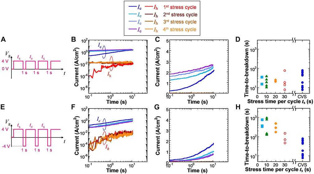
FIGURE 9. (A) Applied voltage scheme with repeating stress of 4 V for time ts and 0 V for 1 s. (B,C) Electron and hole components of gate leakage current at each 4-V stress cycle for ts = 10 s when current is plotted in (B) log scale and (C) linear scale. Between each stress cycle, tests were interrupted by 0 V for 1 s. (D) Total stress time (excluding 0 V interruption duration) before breakdown for different time ts of 4-V stress. (E) Applied voltage scheme when the interrupted voltage is −4 V for 1 s. (F,G) Electron and hole components of gate leakage current at each 4-V stress cycle for ts = 10 s, which were interrupted at -4 V for 1 s between cycles, when current is plotted in (F) log scale and (G) linear scale. (H) Total stress time (excluding −4 V interruption duration) before breakdown for different time ts of 4-V stress.
3.5 Mechanism under voltage stress
The behavior of stress recovery by negative interrupt pulses can be found as well in HfO2 non-ferro-FETs, as shown in Figures 10A, B. These facts suggest that although the leakage current and breakdown voltage of HfO2 non-ferro-FETs and HZO FeFETs are different in detail due to differences in crystallinity or defect density, the fundamental mechanisms of the breakdown and recovery behavior should be generally similar in HfO2-based materials, for instance, same type of defect generation.
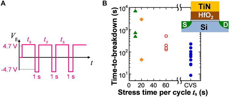
FIGURE 10. (A) Applied voltage scheme with repeating stress of 4.7 V for time ts and −4.7 V for 1 s. (B) Total stress time before breakdown of HfO2 non-ferro-FETs. CVS indicates experiments without recovery pulses.
Considering the above findings, we propose the mechanism under high Vg stress, shown in Figure 11. Typically, SILC as well as noisy gate leakage current (PBD; progressive breakdown) under electrical stress before hard breakdown are attributed to the generation of defects such as oxygen vacancies (Olivo et al., 1988; Rofan et al., 1991; Degraeve et al., 1995; DiMaria et al., 1995). On the other hand, the recovery and repeatable behavior of apparently degraded gate leakage currents observed in FeFETs suggests that the defect redistribution should be the main contribution of apparently degraded characteristics rather than the generation of new defects. These defects are redistributed again after applying an opposite voltage pulse, recovered to the condition close to the initial one before stress. This model is supported by the fact that oxygen vacancies can move during the voltage cycling (Pesic et al., 2016; Florent et al., 2018b). However, if the stress is large enough for defects to move to the condition that triggers hard breakdown, suddenly increasing current generates a huge density of defects, which forms a permanent conduction path and results in the failure of the device. Then, the recovery is no longer available for devices that reach the breakdown condition.
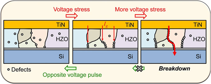
FIGURE 11. Mechanism under electrical stress. The SILC-like behavior is attributed to the redistribution of defects rather than permanent defect generation as recovery is observed. Too much stress will trigger breakdown.
Such a memory operation that the polarization states are frequently switched in a bipolar manner can help extend the device lifetime in terms of breakdown failure. In other words, not only the improvement in the material aspect but also choosing an appropriate memory operation is important for the reliability of FeFETs. Whereas bipolar operation is favorable to improving the breakdown-limited endurance, the memory-window-limited endurance has been reported to have the opposite behavior: memory window narrowing is degraded in a bipolar operation faster than in a unipolar operation (Yurchuk et al., 2014). These findings address that the ideal writing operation on the aspects of breakdown and MW narrowing are different. Thus, the endurance tests for evaluating the real lifetime should be carefully designed. Conventional endurance tests of FeFETs using bipolar stress evaluates only one aspect of device endurance, resulting in underestimation of gate dielectric breakdown and overestimation of MW narrowing.
4 Conclusion
We investigated the behavior of stress-induced degradation and gate dielectric breakdown in FeFETs with ferroelectric HZO as gate dielectrics on Si substrates. It was observed that gate dielectric breakdown in FeFETs is dominated by the breakdown in the HZO layer, not in the IL. Increasing gate and substrate hole currents under stress, due to the defect movement in HZO, were observed before gate dielectric breakdown occurs. These increasing currents are not a permanent phenomenon: Temporary degradation is recovered by applying opposite voltage because of defect redistribution. We found that continuous electrical stress with the same polarity leads to easier hard breakdown, whereas bipolar stress frequently recovers the device distribution and help extend the time-to-breakdown. Because bipolar stress suppresses the breakdown-limited endurance while accelerates the memory window-limited endurance, accurate endurance tests should be carried out to correctly evaluate the endurance characteristics of FeFETs in practical memory operations.
Data availability statement
The original contributions presented in the study are included in the article/supplementary material, further inquiries can be directed to the corresponding author.
Author contributions
KT and ST conceived and proposed the main concepts. KT fabricated devices and characterized the electrical properties. KT, MT, and ST analyzed the data and contributed to the in-depth discussion. KT and ST wrote the manuscript. All authors contributed to the discussions regarding the manuscript.
Funding
This paper is based on results obtained from a project, JPNP16007, commissioned by New Energy and Industrial Technology Development Organization (NEDO) as well as JST CREST Grant Number JPMJCR20C3 by the Japan Science and Technology Agency (JST).
Conflict of interest
The authors declare that the research was conducted in the absence of any commercial or financial relationships that could be construed as a potential conflict of interest.
Publisher’s note
All claims expressed in this article are solely those of the authors and do not necessarily represent those of their affiliated organizations, or those of the publisher, the editors and the reviewers. Any product that may be evaluated in this article, or claim that may be made by its manufacturer, is not guaranteed or endorsed by the publisher.
References
Böscke, T. S., Müller, J., Bräuhaus, D., Schröder, U., and Böttger, U. (2011a). Ferroelectricity in hafnium oxide thin films. Appl. Phys. Lett. 99, 102903. doi:10.1063/1.3634052
Böscke, T. S., MüllerBräuhaus, J. D., Schröder, U., and Böttger, U. (2011b). “Ferroelectricity in hafnium oxide: CMOS compatible ferroelectric field effect transistors,” in Proceedings of the 2011 International Electron Devices Meeting (IEDM), Washington, DC, USA, December 2011, 547–550. doi:10.1109/IEDM.2011.6131606
Chen, I. C., Holland, S., Young, K. K., Chang, C., and Hu, C. (1986). Substrate hole current and oxide breakdown. Appl. Phys. Lett. 49, 669–671. doi:10.1063/1.97563
Degraeve, R., Groeseneken, G., Bellens, R., Depas, M., and Maes, H. E. (1995). “A consistent model for the thickness dependence of intrinsic breakdown in ultra-thin oxides,” in Proceedings of the 1995 IEEE International Electron Devices Meeting (IEDM), Washington, DC, USA, December 1995, 863–866. doi:10.1109/IEDM.1995.499353P
DiMaria, D. J., and Cartier, E. (1995). Mechanism for stress-induced leakage currents in thin silicon dioxide films. J. Appl. Phys. 78, 3883–3894. doi:10.1063/1.359905
Dünkel, S., Trentzsch, M., Richter, R., Moll, P., Fuchs, C., Gehring, O., et al. (2017). “A FeFET based super-low-power ultra-fast embedded NVM technology for 22nm FDSOI and beyond,” in Proceedings of the 2017 IEEE International Electron Devices Meeting (IEDM), San Francisco, CA, USA, December 2017, 485–488. doi:10.1109/IEDM.2017.8268425
Dutta, S., Schafer, C., Gomez, J., Ni, K., Joshi, S., and Datta, S. (2020). Supervised learning in all FeFET-based spiking neural network: Opportunities and challenges. Front. Neurosci. 14, 634. doi:10.3389/fnins.2020.00634
Eitan, B., and Kolodny, A. (1983). Two components of tunneling current in metal-oxide-semiconductor structures. Appl. Phys. Lett. 43, 106–108. doi:10.1063/1.94145
Florent, K., Pesic, M., Subirats, A., Banerjee, K., Lavizzari, S., and Arreghini, A. (2018a). “Vertical ferroelectric HfO2 FET based on 3-D NAND architecture: Towards dense low-power memory,” in Proceedings of the 2018 IEEE International Electron Device Meeting (IEDM), San Francisco, CA, USA, December 2018, 43–46. doi:10.1109/IEDM.2018.8614710
Florent, K., Subirats, A., Lavizzari, S., Degraeve, W., Celano, U., Kaczer, B., et al. (2018b). “Investigation of the endurance of FE-HfO2 devices by means of TDDB studies,” in Proceedings of the 2018 IEEE International Reliability Physics Symposium (IRPS), Burlingame, CA, USA, March 2018. 6D. 3.1-6D.3.7. doi:10.1109/IRPS.2018.8353634
Gong, N., and Ma, T.-P. (2018). A study of endurance issues in HfO2-based ferroelectric field effect transistors: Charge trapping and trap generation. IEEE Electron Device Lett. 39, 15–18. doi:10.1109/LED.2017.2776263
Ichihara, R., Suzuki, K., Kusai, H., Ariyoshi, K., Akari, K., Takano, K., et al. (2020). “Re-examination of Vth window and reliability in HfO2 FeFET based on the direct extraction of spontaneous polarization and trap charge during memory operation,” in Proceedings of the. 2020 Symposia on VLSI Technology and Circuits, Honolulu, HI, USA, June 2020. TF1.2. doi:10.1109/VLSITechnology18217.2020.9265055
Jerry, M., Dutta, S., Kazemi, A., Ni, K., Zhang, J., Chen, P.-Y., et al. (2018). A ferroelectric field effect transistor based synaptic weight cell. J. Phys. D. Appl. Phys. 51. doi:10.1088/1361-6463/aad6f8doi:434001
Kim, S. J., Mohan, J., Kim, H. S., Lee, J., Young, C. D., Colombo, L., et al. (2018). Low-voltage operation and high endurance of 5-nm ferroelectric Hf0.5Zr0.5O2 capacitors. Appl. Phys. Lett. 113. doi:10.1063/1.5052012doi:182903
Kobayashi, K., Teramoto, A., Hirayama, M., and Fujita, Y. (1995). Model for the substrate hole current based on thermionic hole emission from the anode during Fowler-Nordheim electron tunneling in n-channel metal-oxide-semiconductor field-effect transistors. J. Appl. Phys. 76, 3277–3282. doi:10.1063/1.358681
Liao, C.-Y., Hsiang, K.-Y., Lou, Z.-F., Tseng, H.-C., Lin, C.-Y., Li, Z.-X., et al. (2022). “Endurance > 1011 cycling of 3D GAA nanosheet ferroelectric FET with stacked HfZrO2 to homogenize corner field toward mitigate dead zone for high-density eNVM,” in Proceedings of the 2022 Symposia on VLSI Technology and Circuits, Honolulu, HI, USA, June 2022, 393–394. doi:10.1109/VLSITechnologyandCir46769.2022.9830345
Luo, J., Liu, T., Fu, Z., Wei, X., Yang, M., Chen, L., et al. (2022). A novel ferroelectric FET-based adaptively-stochastic neuron for stimulated-annealing based optimizer with ultra-low hardware cost. IEEE Electron Devices Lett. 43, 308–311. doi:10.1109/LED.2021.3138765
Matsui, C., Toprasertpong, K., Takagi, S., and Takeuchi, K. (2021). “Energy-efficient reliable HZO FeFET computation-in-memory with local multiply & global accumulate array for source-follower & charge-sharing voltage sensing,” in Proceedings of the 2021 Symposia on VLSI Technology and Circuits, Kyoto, Japan, June 2021. JFS2-8. doi:10.23919/VLSICircuits52068.2021.9492448
Migita, S., Ota, H., Yamada, H., Shibuya, K., Sawa, A., and Toriumi, A. (2018). Polarization switching behavior of Hf-Zr-O ferroelectric ultrathin films studied through coercive field characteristics. Jpn. J. Appl. Phys. 57. doi:10.7567/JJAP.57.04FB01doi:04FB01
Mulaosmanovic, H., Breyer, E. T., Dünkel, S., Beyer, S., Mikolajick, T., and Slesazeck, S. (2021). Ferroelectric field-effect transistors based on HfO2: A review. Nanotechnology 32. doi:10.1088/1361-6528/ac189fdoi:502002
Müller, J., Böscke, T. S., Schröder, U., Mueller, S., Bräuhaus, D., Böttger, U., et al. (2012). Ferroelectricity in simple binary ZrO2 and HfO2. Nano Lett. 12, 4318–4323. doi:10.1021/nl302049k
Müller, J., Polakowski, P., Müller, S., Mulaosmanovic, H., Ocker, J., Mikolajick, T., et al. (2016). “High endurance strategies for hafnium oxide based ferroelectric field effect transistor,” in Proceedings of the 16th Non-Volatile Memory Technol. Symp. (NVMTS), Pittsburgh, PA, USA, October 2016. doi:10.1109/NVMTS.2016.7781517
Müller, S., Zhou, H., Benoist, A., Ocker, J., Noack, M., Kuzmanov, G., et al. (2021). “Development status of gate-first FeFET technology,” in Proceedings of the 2021 Symposia on VLSI Technology and Circuits, Kyoto, Japan, June 2021. TFS1-5.
Nako, E., Toprasertpong, K., Nakane, R., Takenaka, M., and Takagi, S. (2022). “Experimental demonstration of novel scheme of HZO/Si FeFET reservoir computing with parallel data processing for speech recognition,” in Proceedings of the 2022 IEEE Symposium on VLSI Technology and Circuits, Honolulu, HI, USA, June 2022. doi:10.1109/VLSITechnologyandCir46769.2022.9830412
Ni, K., Sharma, P., Zhang, J., Jerry, M., Smith, J. A., Tapily, K., et al. (2018). Critical role of interlayer in Hf0.5Zr0.5O2 ferroelectric FET nonvolatile memory performance. IEEE Trans. Electron Devices 65, 2461–2469. doi:10.1109/TED.2018.2829122
Olivo, P., Nguyen, T. N., and Ricco, B. (1988). High-field-induced degradation in ultra-thin SiO2 films. IEEE Trans. Electron Devices 35, 2259–2267. doi:10.1109/16.8801
Park, M. H., Lee, Y. H., Kim, H. J., Kim, Y. J., Moon, T., Kim, K. D., et al. (2015). Ferroelectricity and antiferroelectricity of doped thin HfO2-based Films. Adv. Mat. 27, 1811–1831. doi:10.1002/adma.201404531
Peng, H. K., Chan, C. Y., Chen, K. Y., and Wu, Y. H. (2021). Enabling large memory window and high reliability for FeFET memory by integrating AlON interfacial layer. Appl. Phys. Lett. 49, 103503. 671. doi:10.1063/5.0036824
Pešić, M., Fengler, F. P. G., Larcher, L., Padovani, A., Schenk, T., Grimley, E. D., et al. (2016). Physical mechanisms behind the field-cycling behavior of HfO2-based ferroelectric capacitors. Adv. Funct. Mat. 26, 4601–4612. doi:10.1002/adfm.201600590
Rofan, R., and Hu, C. (1991). Stress-induced oxide leakage. IEEE Electron Devices Lett. 12, 632–634. doi:10.1109/55.119221
Schroeder, U., Park, M. H., Mikolajick, T., and Hwang, C. S. (2022). The fundamentals and applications of ferroelectric HfO2. Nat. Rev. Mat. 7, 653–669. doi:10.1038/s41578-022-00431-2
Schuegraf, K. F., and Hu, C. (1994a). Hole injection SiO2 breakdown model for very low voltage lifetime extrapolation. IEEE Trans. Electron Devices 41, 761–767. doi:10.1109/16.285029
Schuegraf, K. F., and Hu, C. (1994b). Metal-oxide-semiconductor field-effect-transistor substrate current during Fowler–Nordheim tunneling stress and silicon dioxide reliability. J. Appl. Phys. 76, 3695–3700. doi:10.1063/1.357438
Shanware, A., Shiely, J. P., Massoud, H. Z., Vogel, E., Henson, K., Srivastava, A., et al. (1999). “Extraction of the gate oxide thickness of N- and P-channel MOSFETs below 20A from the substrate current resulting from valence-band electron tunneling,” in Proceedings of the 1999 IEEE International Electron Device Meeting (IEDM), Washington, DC, USA, December 1999, 815–818. doi:10.1109/IEDM.1999.824274
Sharma, A. A., Doyle, B., Yoo, H. J., Tung, I-C., Kavalieros, J., Metz, M. V., et al. (2020). “High speed memory operation in channel-last, back-gated ferroelectric transistors,” in Proceedings of the 2020 International Electron Device Meeting (IEDM), San Francisco, CA, USA, December 2020, 391–394. doi:10.1109/IEDM13553.2020.9371940
Takayanagi, M., Takagi, S., and Toyoshima, Y. (2001). “Gate voltage dependent model for TDDB lifetime prediction under direct tunneling regime,” in Proceedings of the 2001 Symposia on VLSI Technology Digest of Technical Papers (IEEE Cat. No.01 CH37184), Kyoto, Japan, June 2001, 99–100. doi:10.1109/VLSIT.2001.934968
Tan, A. J., Liao, Y. H., Wang, L. C., Shanker, N., Bae, J. H., Hu, C., et al. (2021). Ferroelectric HfO2 memory transistors with high-κ interfacial layer and write endurance exceeding 1010 cycles. IEEE Electron Device Lett. 42, 994–997. doi:10.1109/LED.2021.3083219
Toprasertpong, K., Lin, Z. Y., Lee, T. E., Takenaka, M., and Takagi, S. (2020a). “Asymmetric polarization response of electrons and holes in Si FeFETs: Demonstration of absolute polarization hysteresis loop and inversion hole density over 2 × 1013 cm−2,” in Proceedings of the 2020 Symposia on VLSI Technology and Circuits TF1, Honolulu, HI, USA, June 2020. doi:10.1109/VLSITechnology18217.2020.9265015
Toprasertpong, K., Nako, E., Nakane, R., Takenaka, M., and Takagi, S. (2022b). Reservoir computing on a silicon platform with a ferroelectric field-effect transistor. Commun. Eng. 1, 21. doi:10.1038/s44172-022-00021-8
Toprasertpong, K., Tahara, K., Fukui, T., Lin, Z., Watanabe, K., Takenaka, M., et al. (2020b). Improved ferroelectric/semiconductor interface properties in Hf0.5Zr0.5O2 ferroelectric FETs by low-temperature annealing. IEEE Electron Device Lett. 41, 1588–1591. doi:10.1109/LED.2020.3019265
Toprasertpong, K., Tahara, K., Hikosaka, Y., Nakamura, K., Saito, H., Takenaka, M., et al. (2022a). Low Operating voltage, improved breakdown tolerance, and high endurance in Hf0.5Zr0.5O2 ferroelectric capacitors achieved by thickness scaling down to 4 nm for embedded ferroelectric memory. ACS Appl. Mat. Interfaces 14, 51137–51148. doi:10.1021/acsami.2c15369
Toprasertpong, K., Takenaka, M., and Takagi, S. (2019). “Direct observation of charge dynamics in FeFET by quasi-static split C-V and hall techniques: Revealing FeFET operation,” in Proceedings of the 2019 IEEE International Electron Devices Meeting (IEDM), San Francisco, CA, USA, December 2019, 570–573. doi:10.1109/IEDM19573.2019.8993664
Toprasertpong, K., Takenaka, M., and Takagi, S. (2022c). On the strong coupling of polarization and charge trapping in HfO2/Si-based ferroelectric field-effect transistors: Overview of device operation and reliability. Appl. Phys. A 128, 1114. doi:10.1007/s00339-022-06212-6
Trentzsch, M., Flachowsky, S., Richter, R., Paul, J., Reimer, B., Utess, D., et al. (2016). “A 28nm HKMG super low power embedded NVM technology based on ferroelectric FETs,” in Proceedings of the 2016 International Electron Device Meeting (IEDM), San Francisco, CA, USA, December 2016, 294–297. doi:10.1109/IEDM.2016.7838397
Weinberg, Z. A., and Fischetti, M. V. (1985). Investigation of the SiO2-induced substrate current in silicon field-effect transistors. J. Appl. Phys. 57, 443–452. doi:10.1063/1.334771
Yan, M.-H., Wu, M.-H., Huang, H.-H., Chen, Y.-H., Chu, Y.-H., Wu, T.-L., et al. (2020). “BEOL-compatible multiple metal-ferroelectric-metal (m-MFM) FETs designed for low voltage (2.5 V), high density, and excellent reliability,” in Proceedings of the 2020 International Electron Device Meeting (IEDM), San Francisco, CA, USA, December 2020, 75–78. doi:10.1109/IEDM13553.2020.9371916
Yurchuk, E., Müller, J., Muller, S., Paul, J., Pesic, M., Bentum, R. v., et al. (2016). Charge-trapping phenomena in HfO2-based FeFET-type nonvolatile memories. IEEE Trans. Electron Devices 63, 3501–3507. doi:10.1109/TED.2016.2588439
Yurchuk, E., Mueller, S., Martin, D., Slesazeck, S., Schroeder, U., Mikolajick, T., et al. (2014). “Origin of the endurance degradation in the novel HfO2-based 1T ferroelectric nonvolatile memories,” in Proceedings of the 2014 IEEE International Reliability Physics Symposium (IRPS), Waikoloa, HI, USA, June 2014. 2E.5.1-2E.5.5. doi:10.1109/IRPS.2014.6860603
Keywords: ferroelectrics, MOSFET, reliability, oxide breakdown, substrate hole current
Citation: Toprasertpong K, Takenaka M and Takagi S (2022) Breakdown-limited endurance in HZO FeFETs: Mechanism and improvement under bipolar stress. Front. Electron. 3:1091343. doi: 10.3389/felec.2022.1091343
Received: 06 November 2022; Accepted: 13 December 2022;
Published: 21 December 2022.
Edited by:
Xiao Gong, National University of Singapore, SingaporeReviewed by:
Quentin Rafhay, Grenoble Institute of Technology, FranceQing-Tai Zhao, Helmholtz Association of German Research Centres (HZ), Germany
Copyright © 2022 Toprasertpong, Takenaka and Takagi. This is an open-access article distributed under the terms of the Creative Commons Attribution License (CC BY). The use, distribution or reproduction in other forums is permitted, provided the original author(s) and the copyright owner(s) are credited and that the original publication in this journal is cited, in accordance with accepted academic practice. No use, distribution or reproduction is permitted which does not comply with these terms.
*Correspondence: Kasidit Toprasertpong, dG9wcmFzZXJ0cG9uZ0Btb3NmZXQudC51LXRva3lvLmFjLmpw
 Kasidit Toprasertpong
 Mitsuru Takenaka
 Shinichi Takagi