 Xu Liu
 Qiumeng Fan
 Zhijie Chen1
 Wei Mao
 Hao Yu
- 1College of Microelectronics, Beijing University of Technology, Beijing, China
- 2School of Microelectronics, Southern University of Science and Technology, Shenzhen, China
Bio-sensors connect the biological world with electronic devices, widely used in biomedical applications. The combination of microelectronic and medical technologies makes biomedical diagnosis more rapid, accurate, and efficient. In this article, the current-mode biosensing front-end integrated circuits (ICs) for nanopore-based DNA sequencing are reviewed and analyzed, aiming to present their operation theories, advantages, limitations, and performances including gain, bandwidth, noise, and power consumption. Because biological information and external interference are contained in extremely weak sensing current, usually at the pA or nA level, it is challenging to accurately detect and restore the desired signals. Based on the requirements of DNA sequencing, this paper shows three circuit topologies of biosensing front-end, namely, discrete-time, continuous-time, and current-to-frequency conversion types. This paper also makes an introduction to the current-mode sensor array for DNA sequencing. To better review and evaluate the research of the state-of-the-art, the most relevant published works are summarized and compared. The review and analysis would help the researchers be familiar with the requirements, constraints, and methods for current-mode biosensing front-end IC designs for nanopore-based DNA sequencing.
1 Introduction
In the combination of bioengineering and integrated circuit technology, the development of accurate current sensing integrated circuits (ICs) is a hot research topic in recent years, especially in the field of biosensing systems, such as ion current detection technology and nanotechnology as shown in Figure 1 (Awan, Wang, Quadir, & Bermak, 2021). This trend of interdisciplinary penetration makes the real-time, sensitive, and robust biosensor system based on CMOS technology more popular (Xu et al., 2019). For instance, the emergence of ICs for DNA sequencing has promoted the research and breakthrough of genetics and has great significance to the prevention of genetic diseases.
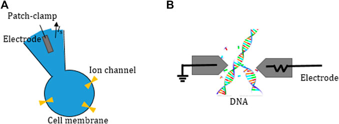
FIGURE 1. Application and field of current sensing and measurement. (A) Ion detection and (B) nanotechnology (Hsu & Hall, 2018).
DNA is a macromolecular polymer composed of deoxynucleotides which can be classified into four classes depending on the base: adenine (A), guanine (G), cytosine (C), and thymine (T). With the discovery of the DNA double helix structure in 1953, exploring DNA sequence and integrity has become a research hotspot all over the world. From 1953 to 1968, DNA sequencing technology was mainly based on a small number of nucleotide fragments and insulin protein (Coulter, 1953). The gene fragments are split and deciphered by optical chromatography or electrophoresis, and the base sequence is deduced from the optimal overlapping fragments (Z. Chen, Burke, & Burns, 2006). In 1977, Sanger and Coulson developed the dideoxy chain termination method, and Gibert and Maxam invented the chemical cleavage method, both of which separated gene fragments by biochemical methods and then used polyacrylamide gel for electrophoresis (Bruno, Alls, & Kiel, 2007). By 1987, Smith, Hood and others initiated the third-generation sequencing technology by single-molecule fluorescent labeling, which could sequence a DNA molecule (up to 1000 bases/day) (Soper, Flanagan, Legendre, Williams, & Hammer, 1996). Although the fluorescence sequencing method made the reading length long and time-consuming, it was greatly shortened when the fluorescence changes are recorded by a microscope. The labeled bases would produce background light, which affected the sequencing accuracy. By 2012, based on Coulter’s idea of using an object in a limited current path to change the resistance, Branton and Deamer proposed for the first time that nanopore sequencing depended on the electrical signal generated when DNA moved through the hole in the membrane (Branton, 2008). This method based on nanopores is deemed as the fourth generation of DNA sequencing.
Compared with previously used sequencing methods using molecular probes and fluorescent labels, nanopore-based DNA sequencing is a label-free approach and meets the high speed and high throughput of DNA sequencing, and its low cost also has made this approach widely concerned and developed in recent years (Stagni et al., 2006; A. Shaghayegh, 2016). The main process of nanotechnology for DNA sequencing is shown in Figure 2. A certain voltage is applied to the nanopores on both sides of the bilayer lipid membranes (BLMs) through electrodes, first. When four bases pass through the nanopores, the equivalent resistances of the four bases are huge (usually at the level of GΩ) and have different blocking effects, which cause a current drop. Therefore, by detecting the change of solution current on both sides of the BLMs and recording the detected base sequence, the purpose of extracting genetic information from DNA can be achieved (Dong, Jiang, Jiang, Huang, & Qin, 2020).
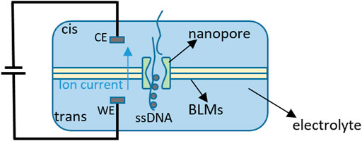
FIGURE 2. Process of nanopore-based DNA sequencing (‘WE’ represents ‘work electrode’ and ‘CE’ represents ‘common electrode’) (Dong et al., 2020).
2 Fundamental and challenges
Although nanopore-based DNA sequencing might have some difficulties in realizing in practice, it is undeniable that the idea of forcing ssDNA to pass through nanopores is very attractive and reasonable. Traditional DNA sequencing methods, such as fluorescent labeling have the disadvantages of limited detection range, lack of specificity, and low sensitivity. In addition, due to the speed of several million bases per second under the effect of an electric field and the slow data collection, the small difference in measuring current between bases makes it very difficult to achieve an acceptable signal-to-noise ratio (SNR) at these timescales (Rosenstein, 2014). In addition, it is also necessary to consider that the thickness of nanopores leads to the passage of four bases simultaneously, which will lead to the low time resolution of the system (Bao, Chen, Peng, & He, 2021). Therefore, the characteristics of high gain and high precision of the biosensing front-end are required.
For the precise current-mode sensor, the front-end ICs mainly include working electrodes and common electrodes inserted in the electrolyte solution, amplifier circuits for converting current, and digital modules for subsequent data processing. The bio-sensor captured current for DNA sequencing is usually at the sub-pA level, accompanied by a dark current of fA to nA and up to μA baseline current (Hsu & Hall, 2018). Thus, it is crucial and challenging to choose an appropriate circuit design with high gain and as low as a few of several fA input-referred noise. Moreover, the translocation rate of the DNA going through the nanopore is about 1–5 μs per base (Zhang, 2012; Bao et al., 2021). Therefore, a circuit with relatively high bandwidth of the order of 1 MHz is needed to detect the current variations. The block diagram of the nanopore-based DNA sequencing system is shown in Figure 3.
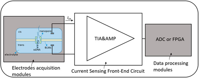
FIGURE 3. Block diagram of the nanopore-based DNA sequencing system.
In this paper, according to the existing current-mode sensing methods for nanopore-based DNA sequencing, the front-end ICs can be divided into three categories, i.e., discrete-time (DT) approach, continuous-time (CT) approach, and current-to-frequency converter. These schemes are mainly based on the realization of a transimpedance amplifier (TIA) with high gain and low noise. The use of a TIA in biomedical applications is an emerging and evolving field and requires in-depth research for the improvement of performance parameters which overcome multidimensional optimization problems. At present, due to its simplicity and a reasonable trade-off between design parameters, the TIA is mainly used in biomedical engineering field and equipment design, such as pulse oximeter, blood glucose meter, blood pressure meter, ECG, and EEG (Atef, Atef, Khaled, & Abbas, 2020; Kumar & Vanita, 2021). The application fields and principles are briefly introduced in Table 1.
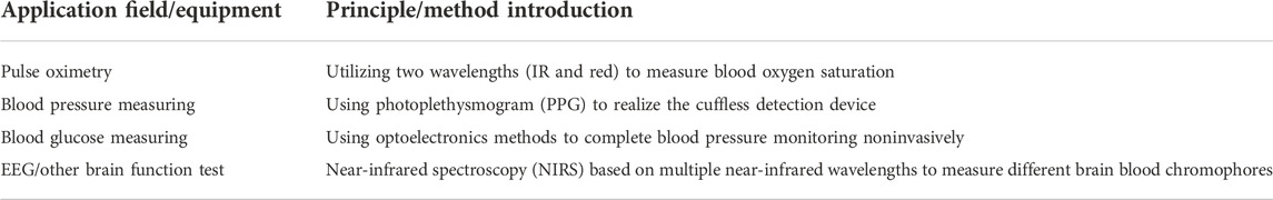
TABLE 1. Applications of TIA in biomedical equipment.
As an analog front-end (AFE) choice for biosensors, we mainly focus on the analysis of TIA design requirements, such as bandwidth, gain, sensitivity, input reference noise, and power consumption, which have a tradeoff with each other and make the choice more challenging. In addition, the front-end ICs with current sensing arrays will also be presented to provide ideas for high-throughput DNA sequencing.
3 Current-mode sensing front end
In the preparation of nanopores, the essence is to reuse the ion channels in biological membranes, such as the derivative nanopores secreted by membrane suspensions named alpha hemolysin (αHL) (X. Liu et al., 2022). Another way is to use solid insulating materials, such as silicon nitride, to prepare solid nanopores, which is relatively stronger than biological nanopores at the signal transmission level.
However, irrespective of the preparation method, the electrolyte solution (i.e., KCL solution) would be divided into cis cavity and trans cavity by film-forming materials. Its nanopore model can be equivalent as shown in Figure 4.
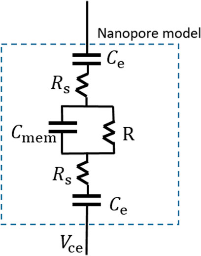
FIGURE 4. Nanopore model (Dong et al., 2020).
3.1 Discrete-time approach-based sensing front ends
According to the principle of DNA sequencing based on nanopores, clamping voltages need to be applied on both sides of the biofilm, which is similar to the patch clamp system used to measure ion channels. As a reference for the amplifier circuit, among the methods of converting precise current, the most direct way is to add resistive feedback elements in the feedback loop of the TIA. The three main feedback methods can be summarized and presented as shown in Figure 5.
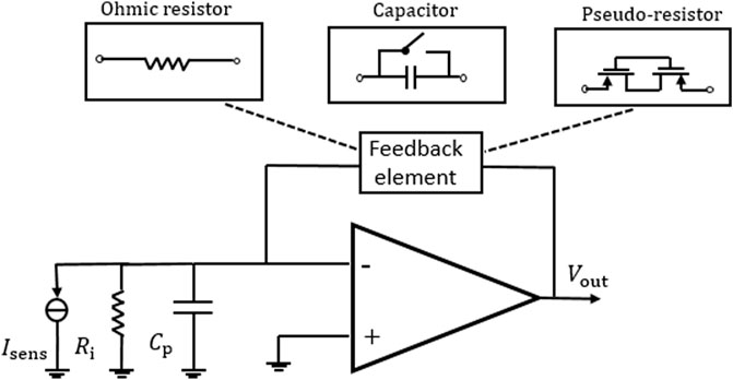
FIGURE 5. TIA with three different feedback elements (Djekic et al., 2017).
Traditional TIAs use ohmic resistance in the feedback loop of the amplifier to realize the conversion of current to voltage. Its output voltage can be approximated as
where
where
In another way, the traditional MOS transistors with weak inversion can be used as high-value pseudo-resistors instead of the traditional ohmic resistor as shown in Figure 5. In this structure, the voltage
The biological sensing signal is extremely weak and easily interfered with by external noise. Another alternative feedback element is a capacitive element, which can not only reduce thermal noise but also improve the tradeoff between gain, bandwidth, and noise, as shown in Figure 5. With this structure, the output voltage of the TIA is an integration of current across a certain amount of time, which is expressed as
where
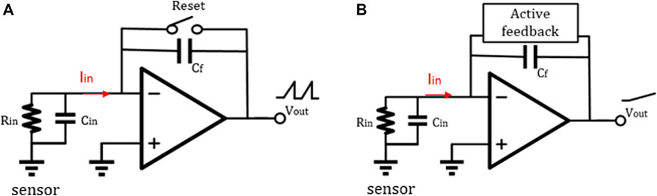
FIGURE 6. (A) TIA with a reset switch and (B) TIA with an active feedback network (Awan et al., 2021).
A typical discrete-time reset model is shown in Figure 6A. By adding a reset switch on both sides of the feedback capacitor, a short periodic reset can discharge the charges accumulated on both sides of the feedback capacitor
In addition, in the DT reset approach, the front-end circuit is easily affected by KCT noise and folded-back high-frequency noise. Therefore, the correlated double sampling (CDS) technique is adopted, thus improving the readout sensitivity (Bennati et al., 2009; Crescentini, Bennati, Carminati, & Tartagni, 2014) (Figure 7). The principle of CDS is to sample the input signal twice. The first sampling is only with low-frequency noise, and the second sampling is the superposition of low-frequency noise and signal. It should be noted that repeated sampling will lead to an increase of overall white noise. To achieve a better noise reduction effect, one good method is to add an anti-aliasing low-frequency filter in the whole system. We summarize and compare the works using DT methods in Table 2.
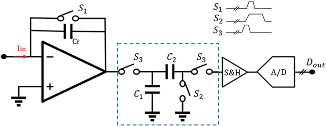
FIGURE 7. General architecture of front-ends using the discrete-time method with CDS (Awan et al., 2021).
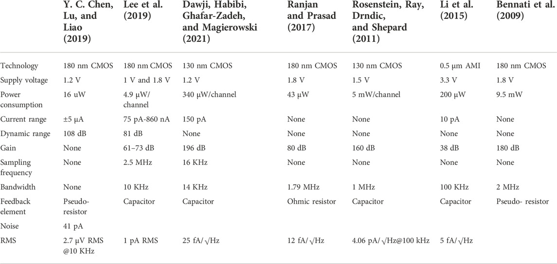
TABLE 2. Performances, comparison, and summary of previous works using the DT approach.
3.2 Continuous-time approach-based sensing front ends
To solve the problem of output saturation in the DT method, in addition to adding a reset switch to periodically reset the capacitor, a second-stage differentiator can also be used to recover the linear relationship between input current and output voltage. This topology uses an integrator-–differentiator structure as shown in Figure 8, and it is called CT approach in this paper.
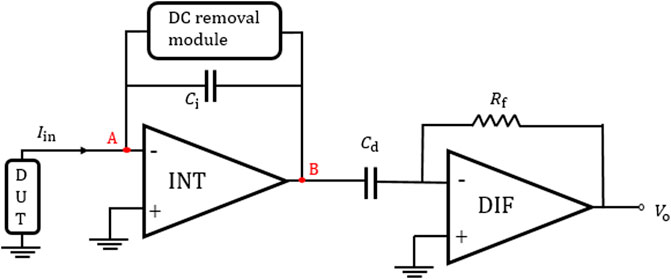
FIGURE 8. Integrator–differentiator structure without continuous-time feedback network (Singh et al., 2019).
This structure mainly consists of an integrator, a differentiator, and an active feedback module. The integrator stage with high gain can produce very low noise density, while the differentiator can ensure a stable and flat frequency response.
The sensing current
Considering the noise performance, the integrator contributes the main input reference noise, and the noise of the differentiator is mostly attenuated by the first stage and thus can be ignored. Therefore, this structure has the advantages of high sensitivity and low noise in a high bandwidth range. In this integrator–differentiator structure, the equivalent input noise power spectral density is
Because
Since the sensing current is often accompanied by a DC signal and the baseline current, an active feedback network is needed to be designed to counteract the DC influence in this integrator–differentiator structure. The establishment of the feedback path is mainly aimed to provide low impedance to attract the DC component of the sensing current and prevent charge accumulation on the plate of the integrating capacitor. Several breakthroughs in reducing noise and improving stability of active feedback networks are summarized in the current research literature. As shown in Figure 9A, the feedback path uses resistor
where A is the loop gain of the operational amplifier. This gain can effectively amplify the signal at low frequencies, but it is strongly attenuated at high frequencies. About concerning |H(0)| >> 1, the DC value at node B in Figure 9A is almost zero regardless of the desired signal, thus ensuring the maximum AC dynamic range of the signal and the high linearity of the integrator under any bias conditions (Ferrari, Gozzini, Molari, & Sampietro, 2009). At |
where, γ is the attenuation of H(s) and its value can be selected by adjusting
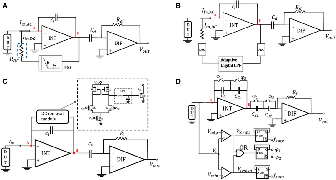
FIGURE 9. (A) Continuous-time approach with R and H(s) as the feedback network (Ferrari et al., 2009), (B) continuous-time approach with an adaptive feedback network (Hsu et al., 2015), (C) continuous-time approach with a differential circuit and low-pass filter (Taherzadeh-Sani et al., 2017), and (D) continuous-time approach with a fixed-threshold window comparator (Dai et al., 2016).
Another feedback network can be implemented by a 12-bit DAC, two LPFs, a 12-bit ADC, and a control logic, as shown in Figure 9B, which composes a hybrid semi-digital (HSD) transimpedance amplifier to transmit these tiny current signals (Hsu, Jiang, Venkatesh, & Hall, 2015). The LPF mainly filters out the high-frequency components in the output of the integrator and feeds the output signal back to the input of HSD-TIA. Therefore,
In the traditional design, the feedback path often uses multiple amplifiers and capacitors, which leads to the introduction of multiple poles and increases circuit complexity. Then, a circuit using a differential pair with diode-connected loads, a low-pass filter (LPF), and an output transistor is adopted as an active feedback path, which can reduce circuit complexity and improve robustness and circuit stability (Taherzadeh-Sani, Hussain Hussaini, Rezaee-Dehsorkh, Nabki, & Sawan, 2017). The schematic diagram is shown in Figure 9C. It is worth mentioning that the feedback loop senses the output of the first stage (
Similarly, in another circuit with a CT approach, a fixed-threshold window comparator is used as the active feedback loop to output one voltage and two frequency outputs (Dai, Perera, Yang, & Rosenstein, 2016), as shown in Figure 9D. Switches
We summarize and compare the performances of the research works using the CT approach by different feedback loops in Table 3. The design comparison of the non-feedback loop is also provided in the table (Singh, Pathania, Sharma, Madan, & Sharma, 2019).
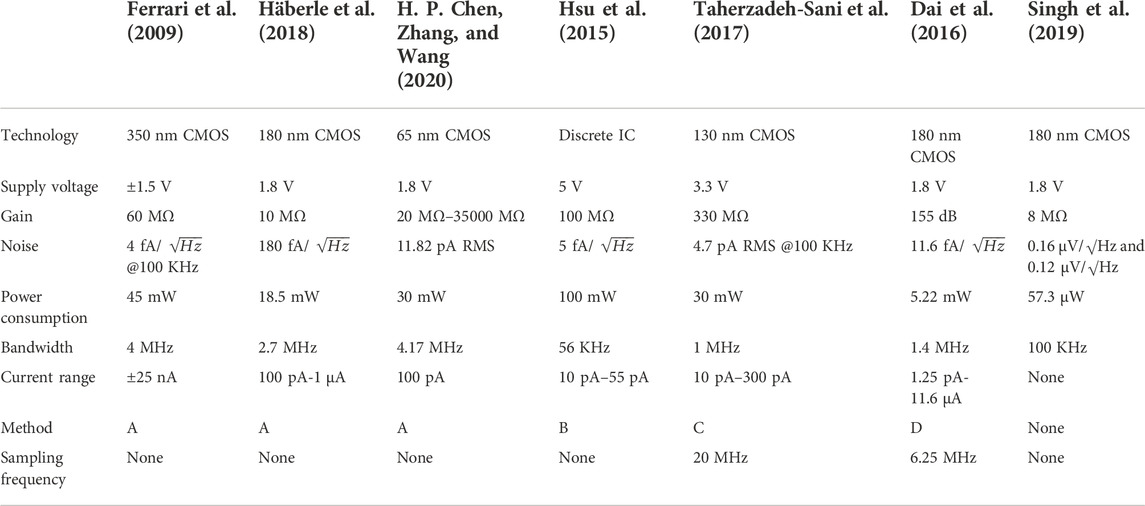
TABLE 3. Performance, summary, and comparison of previous works using the CT approach.
3.3 Current-to-frequency converter-based sensing front ends
In the DT approach- and CT approach-based sensing front ends, most of the structures depend on the relationship between the input current and output voltage. The third type of sensing front end attempts to use the current-to-frequency converter, which converts the current into a time-domain pulse signal with a certain proportional relationship. This structure does not need complex feedback loops to realize DC quantization. Therefore, it is suitable for low power consumption and volume limited equipment, such as implantable medical equipment (Ying & Hall, 2021).
A current-to-frequency (I–F) converter-based sensing front end is shown in Figure 10. After the biological signal is detected by three electrodes at the sensing front end, a potentiostat is used to mirror the sensing current before the I–F converter. In order to minimize the kickback effect between the potentiostat and the I–F converter, the current can be mirrored again between the two circuit modules and appropriately amplified by adjusting the width-to-length ratio of
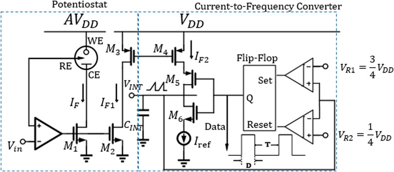
FIGURE 10. Circuit configuration of a current-to-frequency converter (Ahmadi & Jullien, 2009).
Therefore, the mirrored sensing current can be obtained by the ratio of duty ratio D to period T without knowing the values of other factors accurately. In nanopore-based DNA sequencing, in order to explore the differences between the four bases, the ratio of D/T should be less than 1 to facilitate the distinction. In the I–F converter, double comparators comp1 and comp2 are used to form a windowed comparator, and the upper and lower threshold voltages (
In addition to some non-ideal factors from current sources or reference voltages, the propagation delay and offset caused by comparator mismatch will affect the accuracy of D/T and thus cause DC error. However, in the charge and discharge phase, the offset of the comparator is relative, so it has little influence on the linearity of the whole system. The performance summary and comparison of the related works using I–F converters are presented in Table 4.
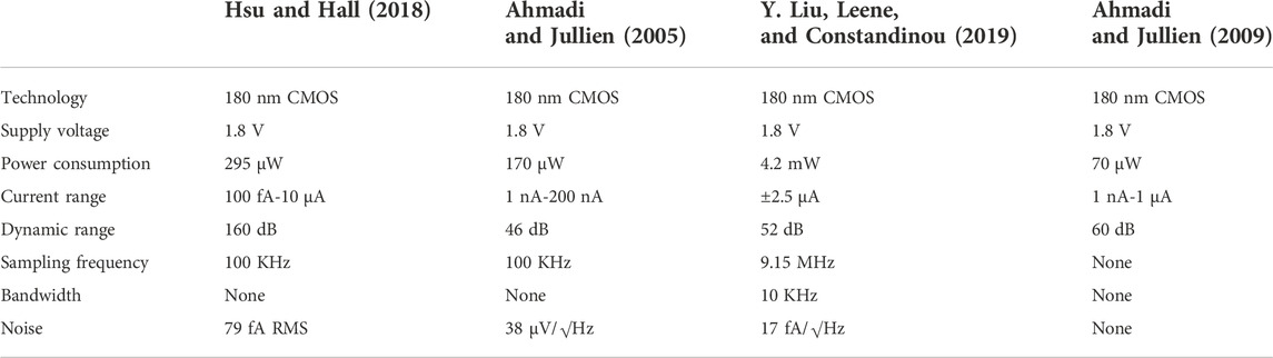
TABLE 4. Performance, summary, and comparison of the I–F convertor-based sensing front ends.
This section explains the choices of current-mode sensing front-end circuit, including the principle and the process of three structures to amplify the weak currents of DNA base. The advantages and disadvantages of the three structures are shown in Table 5 for the reference of designers. It is worth mentioning that designers can further improve or combine these three structures to converge their advantages (Crescentini, Bennati, & Tartagni, 2014).
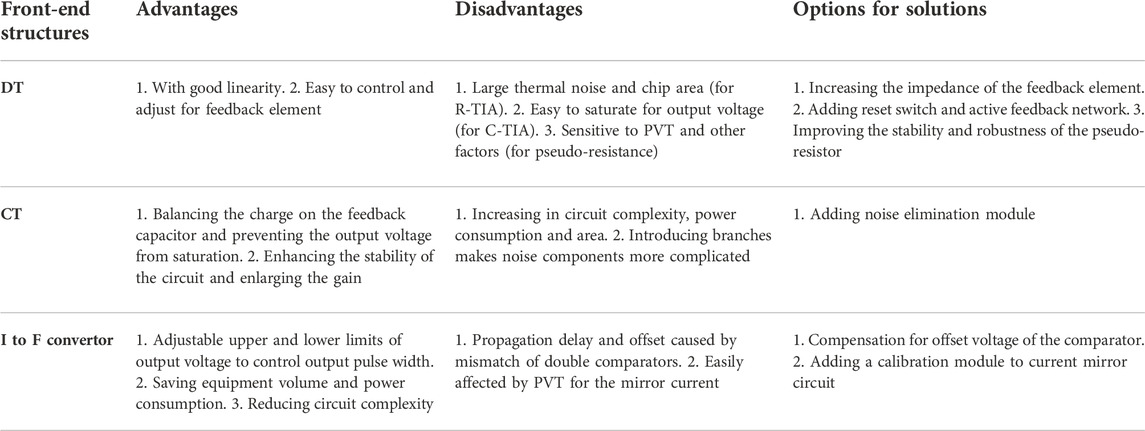
TABLE 5. Comparison of advantages and disadvantages of three current mode front-end structures.
4 Biosensing front-end arrays for DNA sequencing
The aforementioned three types of sensing front ends mainly focus on detecting the sensing current from a single nanopore, but in DNA sequencing, achieving high throughput and high accuracy is the most important purpose. Expanding a single-channel sensing front-end into an integrated biosensor array suitable for large-scale parallel detection can significantly improve the sequencing efficiency and its utility. Although the cost and time of DNA sequencing still need to be broken through, it is undeniable that expanding the measurement flux of DNA and increasing the density of the array are the directions the whole world is striving for. In addition, the DNA sequencing system can also extend its functions completely, such as film-forming detection and subsequent data analysis and processing with the upper computer, which will realize the whole process automatically from transducer preparation to DNA sequencing.
A 90 × 90 fully-electronic biosensor array for nanopore-based DNA sequencing is implemented in a 180-nm standard CMOS process as shown in Figure 11 (Manickam et al., 2012). Pixels of this array adopt 16 μm x 16 μm random bead-array format for DNA loading in which micro-beads deliver DNA strands onto the individual pixels using a flow-through system. The front-end circuit adopts a switched capacitor amplifier circuit and CDS to reduce 1/f noise and deviation. The detection dynamic range of this sensor is 90 dB while consuming 4 mW from a 3.3-V supply when operating at 8.1 s per frame.
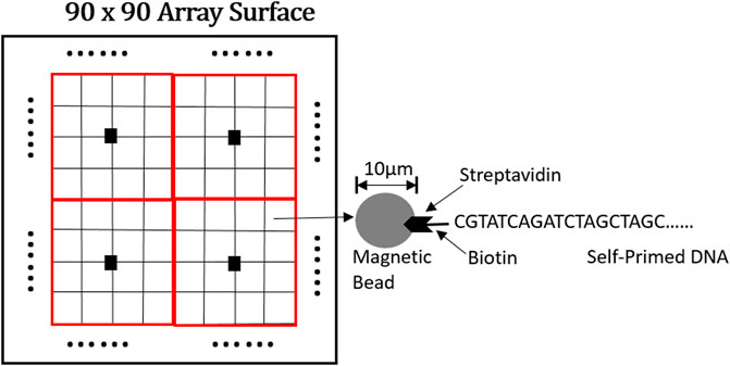
FIGURE 11. Part schematic diagram of a 90 × 90 sensor array interface (Manickam et al., 2012).
In Thei et al. (2010), this design not only integrates a 4 × 3 current-mode sensor array but also adds a microfluidic system to detect the formation of an artificial bilayer lipid film and a readout circuit for data transmission and processing on personal computer (PC) terminals. As shown in Figure 12, the whole system consists of two parts. The first part is a multi-layer interface, which is directly packaged with a current mode ΣΔ converter by a microporous array machined into polyoxymethylene homopolymer (POMH) devices and placed on a printed circuit board (PCB). The second part is a digital signal processing module, which is used to transmit and process data on a PC. The ∑Δ converter adopts the DT approach and has good performance in fast noise shaping. This can output 1 bit digital signal, thus reducing the number of output lines and simultaneously acquiring data from multiple BLMs. The efficiency of DNA sequencing has been greatly improved.
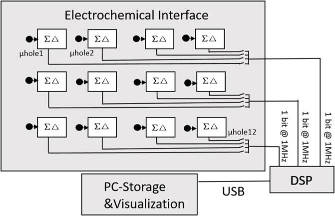
FIGURE 12. System architecture connected to a 4 × 3 sensor matrix of spots (Thei et al., 2010).
To improve the performances in area and power consumption, the amplifier sharing scheme is used (Li, Parsnejad, & Mason, 2015) as shown in Figure 13A. In this article, the front-end array adopts the CT approach in AMI 0.5 μm technology as a selection of amplification for sensing current. In this proposed concept of sharing amplifiers, the pixel-level amplifiers are structures that the non-inverting segments share the same part, while the inverting segments constitute other TIAs. Compared with traditional TIAs, the realization of this structure has a significant improvement in area saving and power consumption. The recording channels of the whole system are divided into N clusters, where each cluster contains four pixel amplifiers, so the area of 400 recording channels is only 0.06 mm2. The system architecture diagram is shown in Figure 13B.
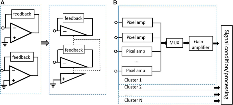
FIGURE 13. (A) Conceptual diagram of sharing OTA as a single pixel unit and (B) system architecture shows that the recording channels are divided into N clusters (Li et al., 2015).
The preparation process and design of nanopore sensor array with higher integration are further introduced (Dong et al., 2020). The platform equipped with a 16 × 8 biosensor array for nanopore detection is also able to perform bilayer lipid membrane capacitance detection and nanopore insertion pulse generation as shown in Figure 14. The front-end array is implemented using the 180-nm CMOS process and mainly composed of a nanopore cell array, decoder modules, readout channels, membrane capacitance detection module, and reference voltage generation module. Each cell consisting of two switches is integrated right under each 10 μm x 10 μm chamber and connected as a 17 × 8 array. Among the whole array, 16 × 8 cells are used for DNA sequencing, while the last row is used for realizing the auto-zero operation of the readout circuit. The whole platform achieves 37.366 µW-per-cell power consumption while occupying 1.633 mm2.
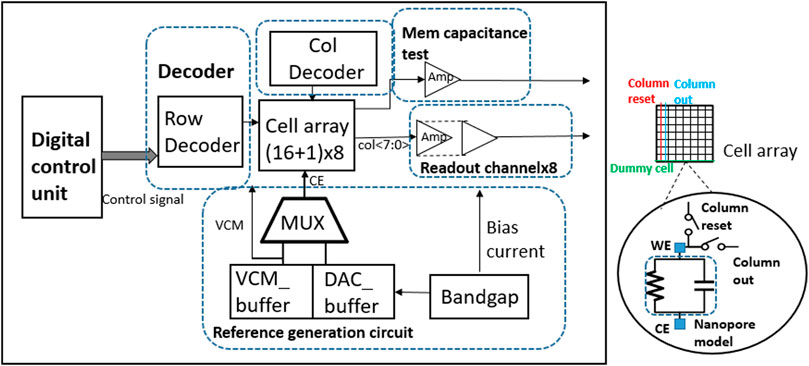
FIGURE 14. System block diagram and cell array architecture (Dong et al., 2020).
In Kumashi et al. (2021), a CMOS sensor array with 256 pixel channels is fabricated based on the 130-nm BiCMOS process, which is used for electrochemical reaction and impedance detection of the biological surface as shown in Figure 15. This sensor array has 16 parallel readout channels, so it can measure high-throughput data quickly and process different samples. The chip contains 2 × 256 working electrodes with a size of 44 μm × 52 μm, 16 reference electrodes with a size of 56 μm × 399 μm and 32 counter electrodes with a size of 399 μm × 106 μm, which together promote the high-resolution screening of test samples. The electrochemical sensing mode of the chip is verified by testing the electrochemical analytes on the biological surface, which shows that the chip can quantitatively generate bioelectric current and distinguish the concentrations of different analytes. In addition, this chip is superior to the conventional discrete setups for exoelectrogen characterization in spatial resolution and detection speed, which is a meaningful step for the combination of chip and bioengineering.
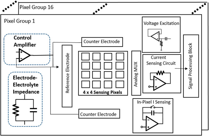
FIGURE 15. Chip architecture of the sensor array with electrochemical and impedance detection module (Kumashi et al., 2021).
The fourth-generation DNA sequencing method has an order of magnitude improvement in speed and cost because it does not need fluorescent labeling. In addition to meeting the requirements of high-speed, high-throughput, and high-precision sensor arrays, breakthroughs should be made in many technical branches, such as nanopore preparation, microfluidic chip, and ASIC, so as to accelerate the commercialization of nanopore sequencing technology. There are two main challenges for multi-channel DNA sequencing arrays. First, the crosstalk and stray capacitance between channels will reduce the signal-to-noise ratio, thus affecting the accuracy of measurement. Therefore, the design of analog front-end with high gain and low noise is the core and key of the whole sequencing system. Second, because the detection array needs high-throughput data processing, we should consider the restriction of chip area and power consumption while expanding the array scale and density and ensure the quantity of detection data as well as the transmission speed. In addition, the influence of other factors on the circuit should be considered when designing the array. For example, the transportation kinetics of a single biomacromolecule is usually faster than the detection time and accompanied by a high DC offset, which poses a significant challenge to the accuracy of detecting weak current (Parsnejad, Li, & Mason, 2016). At present, efforts are being made worldwide to improve the density and detection accuracy of arrays, and many research studies focus on noise reduction technology to improve the detection accuracy. We summarize and compare the performances of the research works achieving biosensing front-end array for DNA sequencing in Table 6.
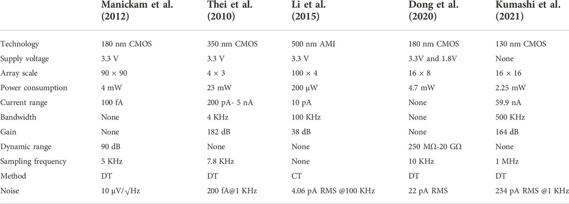
TABLE 6. Performance, summary, and comparison of achieving biosensing front-end arrays.
5 Discussion
Three types of current-mode front-end circuits of DNA sequencing based on nanopores are described in this article, and it is worthwhile to emphasize and discuss the key indicators for the design, which will help the circuit designer improve the chip performance. At the end of this section, we also look forward to the future application of DNA sequencing technology in wearable devices.
Different from the platforms of other amplifier circuits, the biological signals and information on the membrane are carried by an extremely weak sensing current, and the electrodes need to physically contact the two sides of the sensor. Thus, the noise of the whole system has the most serious influence on signal transmission. In addition to the noise caused by the power supply and the capacitances of the contact point, the important noise sources in nanopore-based measurement also include the low-frequency fluctuation of pore conductance and thermally induced fluctuations and high-frequency noise associated with amplifiers and parasitic capacitances. Since most bio-sensing currents are in the order of pA and in several kHz bandwidth, to have good performance in the signal-to-noise ratio (SNR), the input-referred RMS noise should be as low as several hundreds of fA (Crescentini, Bennati, Carminati, et al., 2014). For example, Axon-Axopatch 200B (www.moleculardevices.com), as a patch clamp instrument in bio-electrochemical research applications, has an ultra-low open-circuit noise of 0.13 pA r.m.s at 10 KHz. However, this instrument is very bulky and expensive, and it is still the direction to be overcome to reduce noise for small biomedical integrated circuit chips.
On the other hand, the rapid translocation of DNA through the double-layer artificial lipid membrane and the thickness of the solid-state nanopore result in four bases blocking the nanopore at the same time, which is a challenge to the accuracy and reliability of the whole measurement system (Bao et al., 2021). Many research institutes and companies are constantly improving in different aspects, such as improving time resolution and using biochemical materials to slow down ssDNA.
In recent years, many researchers have focused on the design of the readout circuit of the biosensor system, striving for innovation and breakthroughs in the amplifying circuit and readout circuit. However, to promote the systematization and platform of DNA sequencing, the signal acquisition and subsequent data processing modules of the equipment under test should also be paid attention to, such as the preparation of nanopores, the speed matching of the ADC, and the processing of large amounts of data.
As an emerging technology, the fourth-generation DNA sequencing technology has a significant prospect in the development and potential in the wearable medical devices. DNA base sequencing is an important component and core content of gene detection technology, which is of great significance to the screening and prognosis for gene-related diseases. However, some gene diseases require long-term monitoring and intervention of genes in the body, which makes the combination of gene detection technology and wearable devices become the mainstream trend. For example, in the early screening of cancer, the gene mutation and lysis of diseased tissue cells will occur repeatedly, which requires long-term follow-up detection of cancer cells in patients (Zviran et al., 2020). Thus, the combination of gene detection technology and wearable devices can solve the difficulty of efficient extraction and real-time monitoring of biological macromolecules, which is of great significance to the warning and early screening of related diseases of high-risk groups. At present, some laboratory organizations and companies are committed to the research and development of special nanomaterials and metal microneedle patches, aiming to research the wearable and portable devices for gene detection chips, so as to achieve long-term disease gene monitoring in the human body (Kim et al., 2018; Yang, Kong, & Fang, 2022). Although the fourth-generation DNA sequencing system based on nanopores has only been in existence for more than ten years since this concept was put forward in 2012, it is undeniable that the fourth-generation DNA sequencing system will develop into a platform-based commercial system, which would be used in wearable biomedical systems. In the long run, the combination of gene sequencing technology and wearable devices can not only bring hope to the diagnosis of gene diseases but also promote the combination and development of biomedical engineering and microelectronic technology.
6 Conclusion
This paper summarizes several latest design schemes and circuit structures of current-mode front-end ICs for DNA sequencing. The key design directions of fourth-generation DNA sequencing technology and the directions to be broken through in the future are introduced. Because this technology has the frontier and development potential, we have also summarized and compared the related literatures, which will help circuit designers provide ideas and design directions in the future development of biomedical equipment. (Ca2+-Probe-Based Fluorescence Recording and Electrical Recording).
Author contributions
XL and QF: analysis and arrangement of circuits. PW and ZC: grammar and layout check of the article. XL, QF, WM, and HY: parameter analysis and writing and revising of the manuscript. All authors contributed to the article and approved the submitted version.
Funding
This work is supported by the National Natural Science Foundation of China (NSFC) (Key Program Grant No. 62034007), Shenzhen Science and Technology Program (Grant No. KQTD20200820113051096), and the Program of Beijing Natural Science Foundation (Grant No. 4222062).
Conflict of interest
The authors declare that the research was conducted in the absence of any commercial or financial relationships that could be construed as a potential conflict of interest.
Publisher’s note
All claims expressed in this article are solely those of the authors and do not necessarily represent those of their affiliated organizations, or those of the publisher, the editors, and the reviewers. Any product that may be evaluated in this article, or claim that may be made by its manufacturer, is not guaranteed or endorsed by the publisher.
References
Ahmadi, M. M., and Jullien, G. A. (July 2005). A very low power CMOS potentiostat for bioimplantable applications, 20–24. Proceedings of the Paper presented at the Fifth International Workshop on System-on-Chip for Real-Time Applications (IWSOC'05). Banff, AB, Canada doi:10.1109/IWSOC.2005.32
Ahmadi, M. M., and Jullien, G. A. (2009). Current-mirror-based potentiostats for three-electrode amperometric electrochemical sensors. IEEE Trans. Circuits Syst. I. 56 (7), 1339–1348. doi:10.1109/tcsi.2008.2005927
Atef, A., Atef, M., Khaled, E. E. M., and Abbas, M. (2020). CMOS transimpedance amplifiers for biomedical applications: A comparative study. IEEE Circuits Syst. Mag. 20 (1), 12–31. doi:10.1109/mcas.2019.2961724
Awan, M. A., Wang, B., Quadir, N. A., and Bermak, A. Review and analysis of CMOS current readout circuits for biosensing applications (May 2021). Proceedings of the IEEE international symposium on circuits and systems (ISCAS). Daegu, Korea doi:10.1109/ISCAS51556.2021.9401662
Bao, W., Chen, J., Peng, S., and He, B. (December 2021). Recent advances in DNA biosensors. Proccedings of the Paper presented at the 2021 3rd International Academic Exchange Conference on Science and Technology Innovation (IAECST). Guangzhou, China doi:10.1109/IAECST54258.2021.9695697
Bennati, M., Thei, F., Rossi, M., Crescentini, M., Avino, G. D., Baschirotto, A., et al. (Feb 2009). 20.5 A Sub-pA ΔΣ Current Amplifier for Single-Molecule Nanosensors IEEE International Solid-State Circuits Conference - Digest of Technical Papers,San Francisco, CA, USA 8–12. doi:10.1109/ISSCC.2009.4977451
Branton, D., Deamer, D. W., Marziali, A., Bayley, H., Benner, S. A., Butler, T., et al. (2008). The potential and challenges of Nanopore sequencing. Nat. Biotechnol. 26 (10), 1146–1153. doi:10.1038/nbt.1495
Bruno, J. G., Alls, J. L., and Kiel, J. L. (2007). Feasibility of a DNA-based combinatorial array recognition surface (CARS) in a polyacrylamide gel matrix. IEEE Sens. J. 7 (12), 1609–1616. doi:10.1109/jsen.2007.908501
Ca2+-Probe-Based Fluorescence Recording and Electrical Recording Symposium on VLSI circuits digest of technical papers. 2018 IEEE Symposium on VLSI Circuits Honolulu, HI, USA doi:10.1109/VLSIC.2018.8502322
Chen, H. P., Zhang, L., and Wang, Y. (November 2020). A PVT-robust transimpedance amplifier for ultra-low current sensing. Paper presented at the 2020 IEEE 15th International Conference on Solid-State & Integrated Circuit Technology (ICSICT). Kunming, China doi:10.1109/ICSICT49897.2020.9278389
Chen, Y. C., Lu, S. Y., and Liao, Y. T. (2019). A microwatt dual-mode electrochemical sensing current readout with current-reducer ramp waveform generation. IEEE Trans. Biomed. Circuits Syst. 13 (6), 1163–1174. doi:10.1109/TBCAS.2019.2936373
Chen, Z., Burke, D. T., and Burns, M. A. (2006). International conference of the IEEE engineering in medicine and biology society. Paper presented at the 2006.Imaging Cross-section of DNA electrophoresis in a microfabricated glass device with CLSM Glasgow, UK doi:10.1109/IEMBS.2006.260200
Crescentini, M., Bennati, M., Carminati, M., and Tartagni, M. (2014a). Noise limits of CMOS current interfaces for biosensors: A review. IEEE Trans. Biomed. Circuits Syst. 8 (2), 278–292. doi:10.1109/TBCAS.2013.2262998
Crescentini, M., Bennati, M., and Tartagni, M. (Oct 2014b). IEEE biomedical circuits and systems conference (BioCAS) proceedings, 22–24. Ultra low-noise electrophysiology amplifier on a chip Lausanne, Switzerland doi:10.1109/BioCAS.2014.6981716
Dai, S., Perera, R. T., Yang, Z., and Rosenstein, J. K. (2016). A 155-dB dynamic range current measurement front end for electrochemical biosensing. IEEE Trans. Biomed. Circuits Syst. 10 (5), 935–944. doi:10.1109/TBCAS.2016.2612581
Dawji, Y., Habibi, M., Ghafar-Zadeh, E., and Magierowski, S. (2021). A scalable discrete-time integrated CMOS readout array for nanopore based DNA sequencing. IEEE Access 9, 155543–155554. doi:10.1109/access.2021.3129171
Djekic, D., Fantner, G., Behrends, J., Lips, K., Ortmanns, M., and Anders, J. (September 2017). Esscirc 2017 - 43rd IEEE European solid state circuits conference, 11–14. Leuven, Belgium. A transimpedance amplifier using a widely tunable PVT-independent pseudo-resistor for high-performance current sensing applications doi:10.1109/ESSCIRC.2017.8094530
Dong, C., Jiang, Y., Jiang, K., Huang, Y., and Qin, Y. (October 2020). IEEE international symposium on circuits and systems (ISCAS). Paper presented at the 2020.A 37.37μw-per-cell multifunctional automated nanopore sequencing CMOS platform with 16∗8 biosensor array Seville, Spain doi:10.1109/ISCAS45731.2020.9181095
Ferrari, G., Gozzini, F., Molari, A., and Sampietro, M. (2009). Transimpedance amplifier for high sensitivity current measurements on nanodevices. IEEE J. Solid-State Circuits 44 (5), 1609–1616. doi:10.1109/jssc.2009.2016998
Häberle, M., Djekic, D., Fantner, G. E., Lips, K., Ortmanns, M., and Anders, J. (September 2018). IEEE 44th European solid state circuits conference (ESSCIRC). Paper presented at the ESSCIRC 2018, An integrator-differentiator TIA using a multi-element pseudo-resistor in its DC servo loop for enhanced noise performance Dresden, Germany doi:10.1109/ESSCIRC.2018.8494290
Hong, L., Li, H., Yang, H., and Sengupta, K. (2017). Fully integrated fluorescence biosensors on-chip employing multi-functional nanoplasmonic optical structures in CMOS. IEEE J. Solid-State Circuits 52 (9), 2388–2406. doi:10.1109/JSSC.2017.2712612
Hsu, C. L., and Hall, D. A. (Feb 2018). IEEE international solid - state circuits conference - (ISSCC), 11–15. A current-measurement front-end with 160dB dynamic range and 7ppm INL San Francisco, CA, USA doi:10.1109/ISSCC.2018.8310316
Hsu, C. L., Jiang, H., Venkatesh, A. G., and Hall, D. A. (2015). A hybrid semi-digital transimpedance amplifier with noise cancellation technique for nanopore-based DNA sequencing. IEEE Trans. Biomed. Circuits Syst. 9 (5), 652–661. doi:10.1109/TBCAS.2015.2496232
Kim, H., Jang, H., Kim, B., Kim, M. K., Wie, D. S., Lee, H. S., et al. (2018). Flexible elastomer patch with vertical silicon nanoneedles for intracellular and intratissue nanoinjection of biomolecules. Sci. Adv. 4 (11), eaau6972. doi:10.1126/sciadv.aau6972
Kumar, S., and Vanita, (April 2021). A review of transimpedance amplifiers used in biomedical applications. Paper presented at the 2021 5th International Conference on Computing Methodologies and Communication (ICCMC)., & . Erode, India doi:10.1109/ICCMC51019.2021.9418377
Kumashi, S., Jung, D., Park, J., Tejedor-Sanz, S., Grijalva, S., Wang, A., et al. (2021). A CMOS multi-modal electrochemical and impedance cellular sensing array for massively paralleled exoelectrogen screening. IEEE Trans. Biomed. Circuits Syst. 15 (2), 221–234. doi:10.1109/TBCAS.2021.3068710
Lee, T., Park, J.-H., Cha, J.-H., Chou, N., Jang, D., Kim, J.-H., et al. (2019). A multimodal multichannel neural activity readout IC with 0.7 μW/Channel Ca2+-probe-based fluorescence recording and electrical recording.
Li, H., Parsnejad, S., and Mason, A. J. (Aug 2015). IEEE 58th international midwest symposium on circuits and systems (MWSCAS). Single ion channel CMOS electrochemical instrument for high throughput recording arrays Fort Collins, CO, USA doi:10.1109/MWSCAS.2015.7282111
Liu, X., Song, J., Yang, R., Su, S., Zhang, L., Huang, Y., et al. (2022). Recent advances of biosensors based on split aptamers in biological analysis: A review. IEEE Sens. J. 22 (13), 12460–12472. doi:10.1109/jsen.2022.3176601
Liu, Y., Leene, L., and Constandinou, T. (May 2019). IEEE international symposium on circuits and systems (ISCAS), 26–29. An oscillator based potentiostat with switch-cap feedback for current sensing applications Sapporo, Japan doi:10.1109/ISCAS.2019.8702801
Maitra, R. D., Jungsuk, K., and Dunbar, W. B. (2012). Recent advances in nanopore sequencing. Electrophoresis 33 (23), 3418–3428. doi:10.1002/elps.201200272
Manickam, A., Singh, R., Wood, N., Li, B., Ellington, A., and Hassibi, A. (June 2012). Symposium on VLSI circuits (VLSIC). A fully-electronic charge-based DNA sequencing CMOS biochip Honolulu, HI, USA doi:10.1109/VLSIC.2012.6243822
Parsnejad, S., Li, H., and Mason, A. J. (May 2016). IEEE international symposium on circuits and systems (ISCAS), 22–25. Compact CMOS amperometric readout for nanopore arrays in high throughput lab-on-CMOS Montreal, QC, Canada doi:10.1109/ISCAS.2016.7539187
Ranjan, K. R., and Prasad, R. (April 2017). 1st international conference on electronics, materials engineering and nano-technology (IEMENTech), 28–29. High gain low power low noise trans-impedance amplifier for current sensing application Kolkata, India doi:10.1109/IEMENTECH.2017.8076960
Rosenstein, J., Ray, V., Drndic, M., and Shepard, K. L. (June 2011). 16th international solid-state sensors, actuators and microsystems conference. Nanopore DNA sensors in CMOS with on-chip low-noise preamplifiers Beijing, China doi:10.1109/TRANSDUCERS.2011.5969316
Rosenstein, J. (2014). The promise of nanopore technology: Nanopore DNA sequencing represents a fundamental change in the way that genomic information is read, with potentially big savings. IEEE Pulse 5 (4), 52–54. doi:10.1109/MPUL.2014.2321214
Shaghayegh, A., Zheng, M., Matteo, P., and Anatoly, K. (2016). DNA sequencing by nanopores: Advances and challenges. J. Phys. D. Appl. Phys. 49, 413001. doi:10.1088/0022-3727/49/41/413001
Singh, C. P., Pathania, A., Sharma, K., Madan, J., and Sharma, R. (March 2019). Design of an integrator-differentiator block for a transimpedance amplifier using $0, 23–24. 18\mu \mathrm{m}$ Technology. Paper presented at the 2019 Devices for Integrated Circuit (DevIC). Kalyani, West Bengal doi:10.1109/DevIC45073.2019
Soper, S. A., Flanagan, J. H., Legendre, B. L., Williams, D. C., and Hammer, R. P. (1996). Near-infrared, laser-induced fluorescence detection for DNA sequencing applications. IEEE J. Sel. Top. Quantum Electron. 2 (4), 1129–1139. doi:10.1109/2944.577345
Stagni, C., Guiducci, C., Benini, L., Ricco, B., Carrara, S., Samori, B., et al. (2006). CMOS DNA sensor array with integrated A/D conversion based on label-free capacitance measurement. IEEE J. Solid-State Circuits 41 (12), 2956–2964. doi:10.1109/jssc.2006.884867
Taherzadeh-Sani, M., Hussain Hussaini, S. M., Rezaee-Dehsorkh, H., Nabki, F., and Sawan, M. (2017). A 170-dB $\Omega $ CMOS TIA with 52-pA input-referred noise and 1-MHz bandwidth for very low current sensing. IEEE Trans. VLSI. Syst. 25 (5), 1756–1766. doi:10.1109/tvlsi.2017.2654452
Thei, F., Rossi, M., Bennati, M., Crescentini, M., Lodesani, F., Morgan, H., et al. (2010). Parallel recording of single ion channels: A heterogeneous system Approach. IEEE Trans. Nanotechnol. 9 (3), 295–302. doi:10.1109/tnano.2009.2039489
Xu, W., Wang, B., Duan, M., Ahmed, M., Bermak, A., and Lee, Y.-K. (2019). A three-dimensional integrated micro calorimetric flow sensor in CMOS MEMS technology. IEEE Sens. Lett. 3 (2), 1–4. doi:10.1109/lsens.2019.2893151
Yang, B., Kong, J., and Fang, X. (2022). Programmable CRISPR-Cas9 microneedle patch for long-term capture and real-time monitoring of universal cell-free DNA. Nat. Commun. 13 (1), 3999. doi:10.1038/s41467-022-31740-3
Ying, D., and Hall, D. A. (2021). Current sensing front-ends: A review and design guidance. IEEE Sens. J. 21 (20), 22329–22346. doi:10.1109/jsen.2021.3094830
Zhang, Y. (2012). Combined nanochannel-nanopore device for single-molecule DNA analysis and manipulation. Kyoto, Japan: Symposium on VLSI Circuits Digest of Technical Papers.
Keywords: nanopore, biomedical, current-mode sensor, transimpedance, DNA sequencing, biosensing front-end
Citation: Liu X, Fan Q, Chen Z, Wan P, Mao W and Yu H (2022) A review and analysis of current-mode biosensing front-end ICs for nanopore-based DNA sequencing. Front. Electron. 3:1071132. doi: 10.3389/felec.2022.1071132
Received: 15 October 2022; Accepted: 07 November 2022;
Published: 29 November 2022.
Edited by:
Soumendu Sinha, Central Electronics Engineering Research Institute (CSIR), IndiaCopyright © 2022 Liu, Fan, Chen, Wan, Mao and Yu. This is an open-access article distributed under the terms of the Creative Commons Attribution License (CC BY). The use, distribution or reproduction in other forums is permitted, provided the original author(s) and the copyright owner(s) are credited and that the original publication in this journal is cited, in accordance with accepted academic practice. No use, distribution or reproduction is permitted which does not comply with these terms.
*Correspondence: Wei Mao, d21hbzIzQG91dGxvb2suY29t