
95% of researchers rate our articles as excellent or good
Learn more about the work of our research integrity team to safeguard the quality of each article we publish.
Find out more
REVIEW article
Front. Electron. , 11 October 2021
Sec. Optoelectronics
Volume 2 - 2021 | https://doi.org/10.3389/felec.2021.758603
This article is part of the Research Topic Next Generation Optoelectronics with Emerging Hybrid Materials View all 5 articles
 Vanira Trifiletti1,2*
 Ceyla Asker1Giorgio Tseberlidis2Stefania Riva2Keran Zhao1
 Weidong Tang1
 Simona Binetti2
 Oliver Fenwick1
In recent decades, many technological advances have been enabled by nanoscale phenomena, giving rise to the field of nanotechnology. In particular, unique optical and electronic phenomena occur on length scales less than 10 nanometres, which enable novel applications. Halide perovskites have been the focus of intense research on their optoelectronic properties and have demonstrated impressive performance in photovoltaic devices and later in other optoelectronic technologies, such as lasers and light-emitting diodes. The most studied crystalline form is the three-dimensional one, but, recently, the exploration of the low-dimensional derivatives has enabled new sub-classes of halide perovskite materials to emerge with distinct properties. In these materials, low-dimensional metal halide structures responsible for the electronic properties are separated and partially insulated from one another by the (typically organic) cations. Confinement occurs on a crystal lattice level, enabling bulk or thin-film materials that retain a degree of low-dimensional character. In particular, quasi-zero dimensional perovskite derivatives are proving to have distinct electronic, absorption, and photoluminescence properties. They are being explored for various technologies beyond photovoltaics (e.g. thermoelectrics, lasing, photodetectors, memristors, capacitors, LEDs). This review brings together the recent literature on these zero-dimensional materials in an interdisciplinary way that can spur applications for these compounds. The synthesis methods, the electrical, optical, and chemical properties, the advances in applications, and the challenges that need to be overcome as candidates for future electronic devices have been covered.
The electronic dimensionality of a (semi)conducting material refers to the spatial freedom of electronic charge within it (Xiao et al., 2017). If one or more spatial dimensions are small enough to confine the electronic state wave function, quantum confinement effects are activated. Confinement can occur in one direction, forcing the charge to move in-plane (2D). Charge carriers may be forced to move in only one direction (1D) when two are prohibited. Finally, the confinement can be along all three spatial directions, thus creating a quantum dot (0D), where only discrete energies are allowed. By decreasing the dimensionality, the thermal, optical, electronic, chemical, and mechanical properties are modified. For example, 0D materials have intermediate properties between those typical of discrete molecules and those of bulk semiconductors. The possibility of having easy access to these borderline cases of semiconductor physics pushes their use into a wide range of technological applications. In this extensive review, we want to focus on an emerging class of materials, quasi-zero dimensional halide perovskite derivatives (0D HPds; a list of all abbreviations is given in Table 1). Research on them is in its relative infancy, so the information about them is still incomplete and poorly organised as compared to their 3D counterparts. Often the study of the material is in the context of a specific application, without giving a complete picture of the material properties. With this journey through deposition techniques and emerging applications, we want to spotlight these compounds. They can be deposited rapidly at low temperatures by a variety of methods that are compatible with mass production. 0D HPds are often based on non-toxic elements and have shown higher stability in ambient conditions compared to their 3D halide perovskites (HPs) counterparts. All these features make them attractive for the next generation of HP devices.
TABLE 1. Abbreviations and acronyms used throughout the text.
3D perovskites are composed of a corner-sharing octahedral network with an ABX3 stoichiometry. The highest symmetry structure of the family is tausonite (SrTiO3). However, most exhibit reduced symmetry due to empty sites, lattice distortions, or non-uniformity of chemical composition. As minerals, they are present in nature mainly as oxides, but also as chlorides, silicates, fluorides, and intermetallic compounds. On the other hand, synthetic perovskites are numerous, ranging from organic-inorganic to metallic or metal-free compounds. They can even be synthesized based on noble gases. (Akkerman and Manna, 2020). The halide perovskite subfamily includes standard composition (ABX3) compounds, with divalent B cations (e.g., Pb2+, Sn2+) and A cations of monovalent alkali metals (e.g., Cs+) or organic cations (e.g., CH3NH3+, CH5N2+). Figure 1A shows the various HP groups: cubic halides, antiperovskites, orthorhombic and tetragonal disordered, the vacant BX3, the ordered and the vacancy-ordered HPs (Akkerman and Manna, 2020). The material class has gained tremendous attention due to their unique combination of properties such as high carrier mobility, large absorption coefficient, and long carrier diffusion lengths. They have been widely explored in solar cells, light emitting diodes, sensors, thermoelectric generators, and many other applications (Chen et al., 2015; Park et al., 2016; Sum and Mathews, 2019; Zhang, 2019). The most investigated is the hybrid organic−inorganic perovskite CH3NH3PbI3 for its outstanding photovoltaic performance (Wang R. et al., 2021). Nowadays, lead-based HPs have exceeded the performance of other thin-film single-junction solar cells and have almost reached polycrystalline silicon (Buitrago et al., 2020; NREL, 2020). But still, two factors hinder their commercialization: poor stability and intrinsic toxicity. In addition to device encapsulation, which can partially address the stability issue and may reduce the impact of the intrinsic toxicity, attempts have been made to modify the chemical composition to decrease toxicity and increase stability in air. A low-toxicity class of HPs is obtained by replacing the B site with trivalent cations, such as Sb3+ and Bi3+ (Morad et al., 2019; Bibi et al., 2021). The most investigated compounds are the Bi-based HPs (Zhang L. et al., 2019). The CH3NH3PbI3 band structure, closely related to the 6s2 6p0 electron configuration of Pb2+, underlies the unique properties demonstrated by this compound (Umebayashi et al., 2003; Ganose et al., 2016). By replacing Pb2+ with the much less toxic Bi3+, the ordered vacant perovskite (CH3NH3)3Bi2I9 is obtained (Umebayashi et al., 2003; Hoye et al., 2016; Lyu et al., 2016; Öz et al., 2016). The stoichiometry as well as the 3+ valence state of Bi leads the structure to settle in a quasi-zero dimensional (0D) configuration, where the BiI6 octahedra dimers are fairly isolated from each other (Scholz et al., 2017). Due to the disruption of the 3D perovskite structure of corner-sharing octahedra, they cannot be formerly classed as structural perovskites, belonging instead to the 0D hybrid metal halide group of perovskite derivatives (Xiao et al., 2019; Akkerman and Manna, 2020; Glück and Bein, 2020).
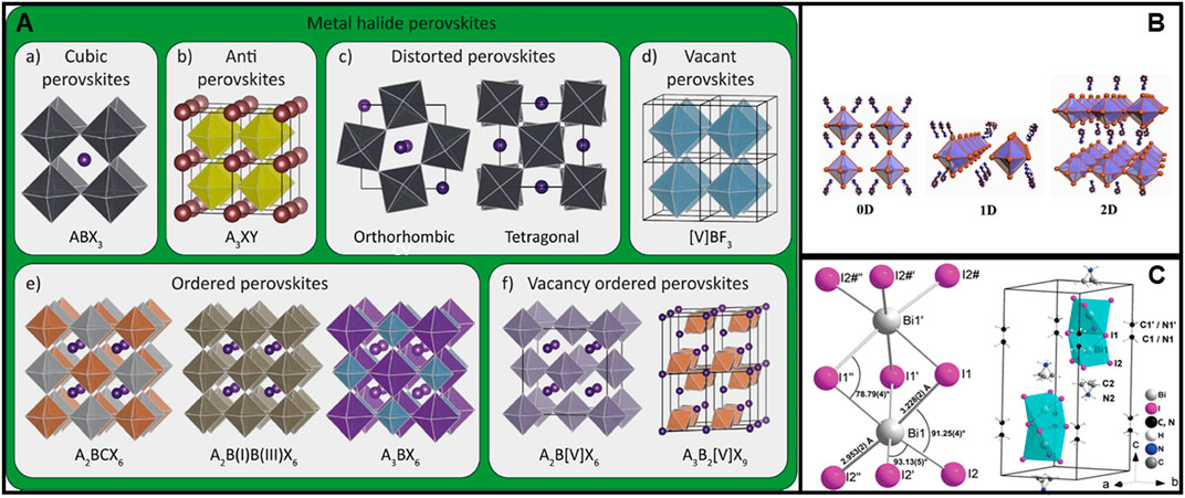
FIGURE 1. (A) HPs groups. Reprinted with permission (Akkerman and Manna, 2020). Copyright 2020, ACS Energy Letters. (B) Low-dimensional HPds structures. Reprinted with permission (Chu et al., 2021). Copyright 2021, Small Structures. (C) (CH3NH3)3Bi2I9 structure and unit cell (Eckhardt et al., 2016). Copyright 2016, Chemical Communications.
Low-dimensional HPds can be obtained either by engineering the crystal geometry (nanoplates, nanowires and nanocrystals) or by tuning the composition and stoichiometry to push the crystal structure into a low-dimensional one (Lin H. et al., 2018; Zhou C. et al., 2019; Zhu and Zhu, 2020; Chu et al., 2021). In this review, we will deal with the latter case because this allows self-assembly in bulk with quantum confinement effects (Lin H. et al., 2018). There is a distinction between electronically low-dimensional materials, where electronic orbital overlap or transport are restricted in one or more dimensions, and structurally low-dimensional materials which exhibit planar, linear or cluster features in their crystal structure. Not all HP-derived materials which are structurally low-dimensional are also electronically low-dimensional, although many are, as discussed by Yan and Mitzi (Xiao et al., 2017). To exploit the physical properties linked to the reduction of (electronic) dimensionality and keep the costs of production processes low is a fundamental requirement to get from lab to market.
Molecular low-dimensional HPds are formed by a periodic distribution of corner-sharing, edge sharing or face-sharing (BX) metal halide octahedra, surrounded by the other cationic (A) component. Octahedra can be arranged in planes, wires, or isolated clusters, forming 2D, 1D or 0D structures, respectively.
Corner-sharing is the most general and it can exist in 0D, 1D, 2D and 3D structures. Edge-sharing occurs only in 0D, 1D and 2D compounds, while face-sharing can only exist in 0D and 1D (Kamminga et al., 2017). The increase in connectivity (corner, edge, face) increases the band gap. This phenomenon has been predicted and measured in (C6H5CH2NH3)2PbI4, which changes the connectivity upon introduction of H2O into the structure. The authors suggest that, although the number of pathways for charge carriers increases with connectivity, they become less favourable (Kamminga et al., 2017). In general, the dimensionality reduction, starting from a 3D compound, happens by substituting the cation A or B so that the lattice structure is distorted. When B is substituted, the distortion mainly affects the B- X–B angle, whose orbital overlap determines the band’s symmetry (Chu et al., 2021). The structure distorts until the stoichiometry changes and the perovskite becomes deficient in order to reach a stable configuration (as in 0D HPds). The energy bands change as a consequence: density-functional theory (DFT) calculations indicate that, when moving from 3D to 0D, the triply degenerate conduction band edge results in optically bright states (Quarti et al., 2020). The Goldschmidt tolerance factor (t), that is an empirical rule defining if a perovskite structure is stable or not, deviates from ideality (Chatterjee et al., 2020). The structure stability is assured with t values between 1.11 and 0.81; (Li et al., 2021b); however, where t is less than 0.9 or greater than 1.0, the structural distortion may lead to different dimensionalities (Hao et al., 2020). Finally, the size of the A cation regulates the interstitial space: for example, a cation such as Cs has a lower confinement effect than an organic cation (Chen D. et al., 2019). Moreover, it also impacts on the distortion and tilting of the metal halide octahedra, therefore indirectly acting on the band structure (Bibi et al., 2021). The octahedra tilting and distortion are therefore due to the cation’s radius and ordering, to the anion’s vacancy and ordering, and, therefore, to the displacement of the central cations in the octahedra, leading to the Jahn-Teller effect (Li et al., 2021b).
Going down in dimensionality from 3D to 0D (Figure 1B), three factors critical for technological applications are affected. The optical bandgap and the excitonic binding energy increase. At the same time, the mobility of the charge carriers and their diffusion length have an increasingly stringent dependence on the crystallographic directions, as the dimensionality is reduced (Chu et al., 2021). In low-dimensional HPds, both Wannier-Mott and self-trapped excitons (STEs) are observed. STEs are generated when the reticular distortion caused by the exciton is so significant as to trap it where it is formed (Zhou C. et al., 2019). These effects can be controlled and exploited, adapting them to the demands of the technological application for which they are designed.
Focus on 0D HPds was rekindled in 2016, when it was discovered that Cs4PbBr6 has a green emission at 520 nm, with a hundred times greater photoluminescence quantum yield (PLQY) than its 3D counterpart. Furthermore, PLQY was not affected by the temperature and remains stable for over a year, even when stored in air (Chen D. et al., 2016). In Cs4PbBr6, the theoretical calculations predict, and transient absorption measurements observe, the generation of small polarons with solid localization in the (PbBr6)4− octahedra and considerable binding energies (Yin et al., 2017). Therefore, 0D HPds properties are expected to strongly depend on the interaction between neighbouring octahedra. For example, the conduction band minimum, a hybrid state between the p orbital of the halide and the s orbital of the metal, depends on the overlap between the neighbouring octahedra (Ju et al., 2018). Cs4PbBr6 has been called a “soft” optoelectronic system, because, following photoexcitation, the structure of (PbBr6)4− octahedra deforms, generating localized polarons, much like in conjugated polymer systems (Almutlaq et al., 2018a).
In general, 0D HPds have isolated anionic metal halide polyhedra surrounded by inorganic or organic cations. This site isolation partially suppresses electronic band formation between metal halide species, enabling the 0D properties. The degree of electronic isolation depends on two main factors: the A cation size that regulates the interstitial space (tuning the octahedra isolation), and the B and X molar ratio defines the stoichiometry (Zhou et al.).
Vacancy ordered perovskites, with 0D character, have chemical formula A3B2X9. A well-studied compound belonging to this family is (CH3NH3)3Bi2I9 (crystal structure in the space group P63/mmc), where bismuth has ligand coordination in a slightly distorted octahedral geometry. The two bismuth atoms are coordinated by three symmetrically equivalent iodine atoms, and the two terminal iodine atoms are located on different specular planes. The two octahedra share a common face and are separated by methylammonium cations. The octahedral distortion comes from the repulsion of the Bi3+ ions (Figure 1C), resulting in the contraction of the bridging I1–Bi1–I1’angle (84°) and the widening of the I2–Bi1–I2’ angle (93°). The anions align with the crystallographic c-axis; the Bi2I93- local structure is displayed together with the unit cell, where the cation and anion positions are highlighted (Eckhardt et al., 2016).
In this review, we will describe the synthesis methods applied so far to 0D HPds, ranging from crystal growth to thin films and pellet fabrication. The synthesis methods are diverse as they have been devised to meet the requirements of a range of device geometries and applications. We will therefore conclude by analysing the applications that have been conceived so far. In addition to the most common optoelectronic applications, we will also review the surprising results reached in the fields of detectors, memristors, capacitors, and thermal energy harvesting.
To increase the quality and the performance of the device in which they are employed, it is essential to achieve a deep understanding of these materials. For this purpose, the synthesis and study of single crystals have been crucial (Chen W. et al., 2020). In fact, in order to investigate their properties on a dimensional scale closer to those required by technological applications, the production of high-quality cm-sized single crystals is one of the researcher’s main motivations. Furthermore, single crystals have fewer defects than thin films, and they can be grain boundary free. Recently, solution methods have been developed to obtain monocrystalline thin films of 3D HPs for use as photodetectors (Zhang J. et al., 2020; Zhang J. et al., 2021). The sizes of 0D HPds crystals are typically smaller than those with higher dimensionalities. In this section, we review the crystal growth methods used to synthesise 0D crystals and discuss the recent developments in these methods to obtain 0D HPds single crystals. We first introduce the solution-based crystallization methods (temperature lowering, and inverse temperature crystallization, solvent evaporation, anti-solvent mediated/solvent layering, solvothermal synthesis and colloidal methods). Then we move to solid-state synthesis, in which we will discuss the crystal growth by Bridgman and mechanochemical synthetic methods.
Solution-based crystallization methods, such as the temperature-lowering method (Dang et al., 2015), inverse temperature crystallization (Saidaminov et al., 2015a; Liu et al., 2015), solvent evaporation (Liao et al., 2015), anti-solvent mediated - solvent layering crystallization (Mitzi, 1999; Shi et al., 2015), solvothermal method (Zhang et al., 2015) and colloidal synthesis (Schmidt et al., 2014), have been developed to obtain high quality HP crystals. The fundamental approach to these methods is based on the formation of supersaturated solutions by adjusting the solubility (Zhang et al., 2020d). The crystallization process, which collects subprocesses such as primary nucleation, crystal growth, secondary nucleation and agglomeration, may start once the supersaturation is achieved (McGinty et al., 2020). Furthermore, the rates of these subprocesses affect crystalline quality, which is crucial for device performance e.g. solar cells (Cheng X. et al., 2020). The solvent, reactants, and temperature impact on the crystal nucleation and growth should be understood and controlled. Herein, we discuss these impacts on 0D HPds with previously reported studies.
The synthesis of 0D HPds by the temperature lowering method dates back over 100 years. The first crystallization of Cs4PbX6 (X = Br, Cl, and I) was performed by Wells et al. in 1893 by cooling down the hot precursor solutions of CsX and PbX2 (Wells, 1893; Thumu et al., 2019). Subsequently, many studies on Cs4PbX6 have been undertaken to control phase purity (Dirin et al., 2016; Zhang H. et al., 2017).
In the temperature lowering method, the crystal size distribution depends on the supersaturation which is the driving force for the nucleation and crystal growth. Meanwhile, the reaction temperature and precursor solubility in the solvent are the two main factors for forming high-quality crystals. In general, a high level of supersaturation at low temperature may be obtained with fast cooling rates. Controversially, slow cooling rates will result in lower supersaturation at higher temperatures, and larger crystals might be obtained as the formation of nuclei-clusters favour the crystal growth (Sánchez et al., 2021). It was reported that, slow cooling process supports the molecule’s rearrangement, leading to a stable structure due to the minimized mass transfer limitations (Maleky et al., 2012). However, the cooling rate needs to be well-determined for each reaction to avoid impurities and small crystals. Likewise, the solubility of each precursor in solvent is crucial to avoid discrepancies and it can be provided by choosing the appropriate solvent for all precursor salts and the temperature range. The synthesis of CsPbBr3 crystals has been reported extensively due to their superior thermal, moisture and light stabilities (Liang et al., 2016; Chen W. et al., 2018). Quan et al. (2017) suggested in their study that water is an excellent solvent for CsBr and PbBr2. However, an additional impurity phase was formed due to the reaction between the metal halide salt and water. Finally, Chen X. et al. (2018) revealed a new slow-cooling strategy: the addition of HBr to improve the solubility of CsBr in dimethyl formamide (DMF) alongside PbBr2 for the growth of centimetre sized CsPbBr3 embedded Cs4PbBr6 crystals. A Cs4SnX6 (X = Cl, Br) crystalline product was synthesized by the slow cooling process, but under inert atmosphere due to tin (II)’s instability and tendency to form tin (IV) compounds under oxidative conditions (Andrews et al., 1983a). Beyond 0D inorganic HPds, organic-inorganic HPds have also been synthesized by this method. (C6H5CH2NH3)3BiBr6 (Chen D. et al., 2020), (C6H5CH2NH3)3SbBr6 (Chen D. et al., 2020) and (C6H5CH2NH3)3InBr6 (Chen D. et al., 2019) were synthesized by dissolving the precursor salts in HBr. After the slow cooling of the solutions to room temperature, centimetre sized crystals were obtained. Similarly, (C6N2H16Cl)2SnCl6 (Song et al., 2020) and (C9NH20)2MnBr4 (Li M. et al., 2019) single crystals were obtained by using an acidic aqueous solution to control the precursor’s solubility. (C6N2H16Cl)2SnCl6 single crystals (100 micro-meter) showed remarkable air and thermal stability at high temperature (270°C). (C9NH20)2MnBr4 single crystal sizes were 5 mm and demonstrated moisture, heat, and light stability. This is despite the structural phase transition observed at 28°C. However, the growth rate is typically low using this method, according to previous studies reported on HPds (Chen Y. et al., 2016; Liu et al., 2018).
Inverse temperature crystallization (ITC) is another efficient method to synthesize HP crystals, where the precursors are dissolved in appropriate solvent and temperature. Increasing the precursor solution’s temperature results in single crystal growth. ITC is time-saving compared to some other solution-based methods. For instance, Saidaminov et al. (2015b) proposed a novel method based on retrograde solubility enabling 3D CH3NH3PbX3 mm-sized single crystals to grow faster than previously reported growth methods. ITC works well with those materials that are highly soluble at room temperature and become sparingly soluble with increasing the solution temperature (Dang et al., 2016). However, there are several limitations to this method that can affect the quality of single crystals. First, the use of organic solvents such as DMF and dimethyl sulfoxide (DMSO) can result in intermediate adduct phase generation (Hao et al., 2014; Hao et al., 2015; Petrov et al., 2017; Petrov et al., 2020) such as (CH3NH3)2Pb3I8·2DMF and (CH3NH3)2Pb3I8·2DMSO due to the strong interactions between organic solvents and precursors. Annealing can be used to remove these by-products, but introduces an extra step into the process (Rong et al., 2015). Second, it is challenging to maintain the same growth rate throughout the whole growth process. The growth rate falls as the solute concentration decreases at a fixed temperature. As a result, it may lead to structural imperfections due to specie’s different diffusion behaviour and also smaller single crystals (Wang W. et al., 2020). This method has been extended to the preparation of 0D HPd systems, as well. For example, pure 0D Cs4PbBr6 nanocrystals were obtained after the purification process performed by Saidaminov et al. (2016) They found that CsBr/PbBr2 precursor solutions in DMSO at 120°C produce Cs4PbBr6 nanocrystals with some CsPbBr3 traces. More interestingly, unlike Cs4PbBr6 nanocrystals, CsPbBr3 nanocrystals were soluble in DMSO. Thus, they collected Cs4PbBr6 nanocrystals formed at 120°C and washed them with DMSO to remove CsPbBr3 and obtain a pure Cs4PbBr6 phase illustrated in Figure 2A.
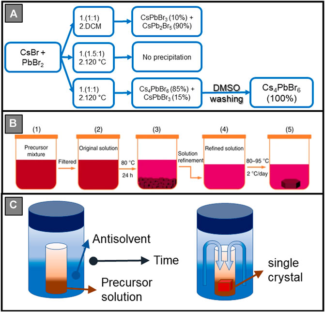
FIGURE 2. (A) Synthesis and purification of Cs4PbBr6. (B) Schematic of the nucleation-controlled ITC method to grow Cs3Bi2I9. Reprinted with permission (Zhang et al., 2020c). Copyright 2020, Nature. (C) Schematic diagram of anti-solvent diffusion crystal growth.
Unlike 3D HP crystals, the size of 0D crystals formed by ITC is limited to the nanometre to micron range. Nevertheless, Zhang et al. (2020c) reported a new approach to retrograde synthesis, the so-called nucleation-control growth method (Figure 2B), to overcome this limitation. They developed this method to synthesise centimetre-sized Cs3Bi2I9 crystals by removing extraneous nucleation seeds midway through the process, including dust, bubbles, particulates, defects, and container surface scratches (Volmer, 1926; Ford, 1997). Sub-millimetre reddish-brown Cs3Bi2I9 crystallites were obtained on the bottom of container after the solution was heated to 80°C. They removed after 24 h, and the upper portion is transferred into another container for growing large crystals. The explanation for the thermodynamics of the nucleation-controlled method to grow Cs3Bi2I9 single crystals follows the classical nucleation theory (Volmer, 1926; Ford, 1997). The spontaneous growth of crystallites or precipitates will occur if the sites with radius r are larger than the critical nucleation radius r0, (r > r0). As the growth process continues, crystallites will merge into a continuous solid. However, by eliminating extraneous nucleation sites, only several large high-quality single crystals can be harvested (Zhang et al., 2020c). They started the process by dissolving a stoichiometric ratio of the precursors in a mixed solvent (DMF/DMSO). Sub-millimetre Cs3Bi2I9 crystallites were precipitated after careful filtration followed by heating. After the solution refinement process, where the upper portion of the solution is transferred into another container, the solution was heated from 80°C to 95°C at a ramp rate of 2°C per day. A large Cs3Bi2I9 single crystal with a dimension of 12 mm × 12 mm × 3 mm was obtained after several days. Despite the long procedure, this method remains one of the best for growing large 0D single crystals. Similarly, Liu et al. (2020c) synthesized CH3NH3Bi2I9 large single crystals with a dimension of 26 mm × 26 mm x 8 mm by eliminating nucleation seeds. For the first time it has been possible to synthesize single inch (about 3 cm) lead-free crystals with satisfactory environmental stability. This was attributed to structural stability and elimination of solvent residues, grain boundaries, inclusions, and voids within the crystals. Very recently, Xu et al. (2021) reported high quality centimetre-sized Cs4PbI6 single crystal synthesised by a similar method. Cs4PbI6 precursor solution (0.5 M) was prepared by dissolving CsI and PbI2 in a mixed solvent (DMF/DMSO = 4/1) with a molar ratio of 4:1 at 50°C for 24 h. Then, the precursor solution was filtered using a polytetrafluoroethylene (PTFE) filter with 1.5 μm pore size. After that, the precursor solution was heated to 75°C with a 0.2°C/h rate and was kept at this temperature for several days. Finally, the high-quality Cs4PbI6 perovskite single crystal was harvested from the solution (Xu et al., 2021).
In solvent evaporation crystallization, precursors with desired molar ratio are mixed in a suitable solvent, which is then slowly evaporated. During solvent evaporation, the precursor concentration gradually increases, eventually reaching the supersaturation conditions needed for crystal growth. As one of the most straightforward techniques for single crystals growth, solvent evaporation has been adopted to fabricate both organic-inorganic and all-inorganic perovskites (Dou et al., 2015; Chang et al., 2018). This method has the advantage of broad applicability and ease of operation. For instance, Hua and coworkers (Hua et al., 2019) used trimethyliodomethylammonium chloride (TMIM·Cl) and SnCl4·5H2O aqueous solution (molar ratio 1:2) to synthesize hybrid organic-inorganic [TMIM]2SnCl6 through solvent evaporation. The colourless block crystal had a 0D HPd-like crystal structure and good purity with an X-ray diffraction (XRD) result highly consistent with the simulated material. In 2020, Zhang and co-workers (Zhang F. et al., 2020) used this strategy to synthesise all-inorganic 0D Cs3Cu2I5 which other groups failed to fabricate using vapour saturation of an antisolvent (Chen H. et al., 2020). In this work, CsI and CuI powders (molar ratio 3:2) were dissolved in DMF under a short duration ultrasonic treatment and allowed to evaporate overnight. The obtained crystal was millimetre-sized. The work also noted that larger crystals could be obtained by using a solution with higher precursor concentrations.
In some cases, the desired low-dimensional material is unstable in the precursor solvent. Wang and colleagues (Wang Y. et al., 2021) faced the issue by tuning the solvent mixture. In this work, 0-D (CH3NH2CH3)4PbI6 single crystals were fabricated by solvent evaporation of PbI2 and CH3NH3I (molar ratio 1:4) dissolved in DMF. Hydroiodic acid and a small amount of phosphoric acid were added to the solution and stirred for hours. Notably, DMF serves as a solvent and reacts with hydroiodic acid to form CH3NH2CH3+ molecules. The (CH3NH2CH3)4PbI6 single crystals grew through this supersaturation and presented good purity. Hydrohalic acids therefore serve both as reactants and promoters of halogenation. A similar strategy was used by Yangui and co-workers (Yangui et al., 2019) to synthesize two 4-aminopyridinium (4AMP)-based hybrid organic-inorganic materials, namely (C5H7N2)2HgBr4·H2O and (C5H7N2)2ZnBr4. Hydrobromic acid, equimolar with MBr2 as MBr2 (M = Hg, Zn) precursors, was added to the solution to improve crystal quality. The stability of the two single crystals was reported: the former material remained stable for several weeks, but the crystallinity slightly decreased over time, and impurity peaks in both crystals became detectable after 1–2 months. Solvent evaporation can be time-consuming compared to other methods. In Wang’s report (Wang Y. et al., 2021), the crystal appeared after 2 weeks and was collected after a month. The solution volume is also a key parameter to be controlled.
Anti-solvent mediated crystallization method is one of the most common methods used to grow HP single crystals. As in other solution-based methods, supersaturation is a driving force for the nucleation process. It can be easily accomplished by exposing a homogeneous solution to another solvent (anti-solvent) in which the desired product has poor solubility, as illustrated in Figure 2C (Konstantakou et al., 2017). It should be considered that the choice of the solvent/anti-solvent, the volume ratio, diffusion time and temperature are important parameters for the approach’s efficacy. For example, using alcohol, i.e., isopropanol as anti-solvent, may result in solute-solvent (organic salt-alcohol) hydrogen bond interactions as discussed by Shi et al. (2015) Furthermore, increasing the volume of anti-solvent can reduce the crystal size. Zhou et al. (2018d) used anti-solvent diffusion methods to synthesise 0D (Ph4P)2SbCl5 crystals. DMF (1 ml) and diethyl ether (2 ml) were used as solvent/anti-solvent pair. They investigated increasing the amount of anti-solvent, finding that this resulted in faster crystallization but reduced crystal size. They also performed rapid crystal growth in which crystal’s growth is initiated by injecting anti-solvent into the precursor solution. Precursors and solvent co-crystallize during the growth process, going through a metastable structure. The phase transition is completed when the solvent is removed, giving almost identical crystals to those prepared by the slow vapour diffusion technique. As aforementioned, ITC of Cs4PbBr6 requires an additional purification step to eliminate the CsPbBr3 phase and obtain pure Cs4PbBr6. On the other hand, De Bastiani et al. (2017) synthesised pure Cs4PbBr6 single crystals without further purification. Diethyl ether acts as an anti-solvent that diffuses into the precursor solutions in DMSO at room temperature due to its low boiling point and high vapour pressure. 500-μm crystals were obtained after 2 days. However, more time spent on crystallization could result in larger crystals. In the same year, Cha et al. (2017) also reported the single crystal growth of Cs4PbX6 by the anti-solvent method. The single crystals with a dimension of 0.56 × 0.39 × 0.32 mm3 were obtained after 4 days by injecting HBr solution into the precursor solutions in DMSO. Using an analogous method, Cs3Cu2I5 lead-free inorganic HPd single crystals with a size of 5 mm can be prepared by diffusing methanol (MeOH) into the precursor DMSO solution (Jun et al., 2018). Zhou et al. (2018c) prepared pure and uniform single crystalline (C4N2H14X)4SnX6 (X = Br or I) by diffusing dichloromethane (DCM) into DMF or gamma-Butyrolactone (GBL) precursor solutions at room temperature under inert atmosphere. Additionally, they grew (C9NH20)2SbCl5 single crystals by using acetone as anti-solvent and DMF precursor solutions. (Ph4P)2MnCl4 single crystals were prepared by the same group by diffusing diethyl ether into the DMF precursor solutions (Ben-Akacha et al., 2020). Likewise, other organic-inorganic 0D HPds, containing Bzmim (1-benzyl-3-methylimidazolium), such as (Bzmim)2SbCl5 (Wang et al., 2019b), (Bzmim)3SbCl6 (Wang et al., 2019b), (C9NH20)2SnBr4 (Zhou et al., 2018b), (PPN)2SbCl5 (He et al., 2020) and (C38H34P2)MnBr4 (Xu L. J. et al., 2020) single crystals (in millimetre to centimetre size scale) could be synthesized in the presence of anti-solvent (Bzmim)2SbCl5 (Wang et al., 2019b) and (Bzmim)3SbCl6 (Wang et al., 2019b) were also synthesized by the temperature lowering method. The benzene ring in the Bzmim+ cation is electron-rich, and p-π interactions improved the stability of the compounds. In specific cases, additional metal halide salts can be added to increase the quality of the crystals. Lin et al. (2019) reported the large single crystal growth of 0D (C13H19N4)2PbBr4 where ZnBr2 was added before the anti-solvent (DCM) diffusion. Though the reaction mechanism is unknown, it is believed that surface defects may be reduced in the presence of bromide, or ZnBr2 crystals may act as seeds or templates to assist the crystal growth. Without ZnBr2, only low-quality (C13H19N4)2PbBr4 crystals were obtained.
Another strategy to grow the HP single crystals is the solvent-layering method, where the crystal grows at the interface between immiscible solvents. This method exploits the different solubility of the material in the two solvents (Dang et al., 2016). Mitzi et al. (Mitzi, 1999) synthesized 2D dimensional (C6H5C2H4NH3)2PbCl4 single crystals by adding methanol into the PbCl2 precursor solution in H2O/HCl followed by addition of the organic salt, C6H5C2H4NH2. Lately, 0D (BA)3Bi2I9 (BBI) (where BA is benzylammonium) single crystals were synthesized by Pious et al. (2020) BBI crystals were formed by dissolving BiI3 in HI and benzyl ammonium iodide in methanol; the two solutions form separate layers when they are poured in a glass vial, and mm-sized rod-shaped crystals were obtained in several hours. This novel HPd was developed by introducing an aromatic benzylammonium cation with greater polarizability and conductivity (due to the delocalization of electronic wave function) than alkyl group cations. Similarly, (Bmpip)2GeBr4 (where Bmpip is 1-butyl-1-methylpiperidinium) crystals were also synthesized via this method. Diethyl ether was carefully layered onto precursor solutions in ethanol and single crystals formed at the interface (Morad et al., 2019). However, (Bmpip)2GeBr4 decomposed in 1 day due to Ge(II) oxidation after exposing to ambient atmosphere.
Another solution-based strategy used for the synthesis of 0D HPd single crystals is the solvothermal method. The chemical reaction of precursor salts and solvent occurs in a closed system (an autoclave) at high temperature and pressure. The usability of both aqueous and nonaqueous solvents such as water (hydrothermal), alcohol, acidic aqueous solutions, carbon dioxide, organic and inorganic solvents makes this method suitable for crystal growth (Shaikh et al., 2020). However, in many reports, the term “hydrothermal” describes all types of synthesis that occurs in a closed vessel with controlled temperature and pressure (Xu et al., 2015). The crystallization process takes place via a slow cooling process.
Furthermore, it may be advantageous for materials decomposed by air (tin and germanium) as the crystallization of dissolved material happens in a sealed autoclave at elevated temperature and pressure. Though it is possible to obtain the product with high purity and crystallinity, high temperature and pressure may result in crystal disorder as the characteristics of a solvent, such as viscosity, are strongly dependent on temperature and pressure (Arya et al., 2020). Cs2InBr5.H2O 0D single crystals were synthesized by Zhou L. et al. (2019). Precursor salts were dissolved in HBr solution at 130°C. Subsequently, the mixture was transferred into a Teflon autoclave and sealed in a stainless-steel Parr autoclave. The slow cooling process led to 2 mm-sized crystals. Other 0D Rb-based inorganic HPds such as Rb7Bi3Cl16 (Xie et al., 2019) single crystals were synthesized in the presence of acidic aqueous solvent with size dimensions of 18.4 × 7.2 × 6.0 mm. Apart from inorganic HPs, organic-inorganic HP single-crystal could also be synthesized with this method (Takeoka et al., 2005; Chen X. et al., 2018; Sun et al., 2020). Recently, 0D tin-based organic HPd single crystals (C8H14N2)2SnBr6 (Su B. et al., 2020) were grown in an autoclave by the temperature lowering method. The 2-cm-size single crystals with excellent air stability were obtained after 3 weeks. The use of benzene ring in C8H14N22+ cation composition improved the degree of organic cation rigidity.
Colloidal HPs have received huge attention due to their high photoluminescence quantum yields (PLQY) (Ma et al., 2018). Colloidal synthesis methods are widely used in the fabrication of quantum dots (QDs) which are considered geometrical 0D nanostructures or nanoparticles based on 3D ABX3 structures (Lin H. et al., 2018; Pu et al., 2018). Colloidal synthesis methods offer various precursors to choose from, and the ratios are not necessarily limited to stoichiometry (Tan et al., 2020). Several strategies have been proposed to prepare HP nanocrystals with controlled size, shape, and quality. One of them is the liquid-phase bottom-up strategy which is proven as one of the best routes for high-quality nanocrystal synthesis. The hot-injection method, ligand-assisted reprecipitation (LARP) and reverse microemulsion methods are used to synthesise 0D nanocrystals. Hot-injection or the organometallic high-temperature colloidal method (Wu et al., 2011) is based on a precursor injection into a hot solution containing other precursors, organic ligands and a high boiling solvent. Though it is one of the most common techniques, this method’s main requirements are high temperature and an inert atmosphere. For example, Cs4PbX6 (X = Br, Cl, I) (Akkerman et al., 2017) and Cs4SnX6 (X = Br, I) (Tan et al., 2020) nanocrystals were synthesized by the hot-injection method.
For the synthesis of Cs4PbX6 (X = Br, Cl, I), PbX2 was dissolved in octadecene, oleic acid and oleyamine and heated to 100°C. At the same time, CsCO3 was dissolved in oleic acid and heated to 150°C. When the temperature reached the optimal value for each halide, the precursors were injected swiftly. Cs4PbX6 nanocrystals were obtained with tenable sizes ranging from 10 to 36 nm. Liu Z. et al. (2017) proposed a two-step dissolution-recrystallization mechanism for the transformation of CsPbBr3 into 0D Cs4PbBr6 in the presence of oleylamine and alkyl-thiol. This two-step mechanism was realized via the hot-injection method followed by decomposition of CsPbBr3 and formation of Pb2+-thiol complexes where alkyl-thiol ligands improved the size uniformity and chemical stability of the derived Cs4PbBr6 nanocrystals. In the last years, the interest in the synthesis of lead-free nanocrystals has increased such that Yang et al. reported the facile synthesis of cubic shaped Cs3BiX6 (X = Cl, Br) nanocrystals (NCs) via a hot-injection method using benzoyl halides as halide precursors. The size of Cs3BiCl6 NCs tuned from 9.8 ± 1.3 to 6.9 ± 0.9 nm by decreasing the reaction temperature from 160 to 140°C. The studies demonstrated the thermal stability of these NCs up to 200°C without crystal structural degradation. Moreover, this study proves the ability of Cs3BiX6 NCs to transform into other bismuth-based HPd-analogues via facile anion exchange or metal ion insertion reactions. NCs of another lead-free 0D HPd Cs4SnBr6 with an average size of about 20 nm were synthesized by Chiara et al. (2020), showing superior stability in air for more than 96 h, compared to an analogous CsSnBr3 3D HP nanocrystals that showed stability for only a few minutes.
On the other hand, hot injection synthesis is highly sensitive to reaction temperature such that products with different dimensionalities can be obtained. For instance, Cheng et al. (2019) performed a synthesis at different temperatures. Cs3Cu2I5 nanocrystals were obtained at 70°C by reacting a Cs-oleate precursor with Cu(І)-halide in octadecene. However, when the temperature was increased to 110°C, the products were 1D CsCu2I3 nanorods.
Ligand-assisted reprecipitation (LARP) is another colloidal technique where high-quality nanocrystals can be obtained in an ambient atmosphere and at room temperature. The precursor solution containing organic ligands (oleyamine, oleic acid) dissolved in a solvent such as DMF, DMSO or GBL, is injected into solvents in which the precursors are poorly soluble like toluene, hexane, or ethanol. The mixture of these two solvents triggers nucleation and crystal growth. The precursor to ligand ratio can control the nucleation and growth of nanocrystals (Shamsi et al., 2019). Rb7Bi3Cl16 single crystals can be grown by solvothermal reaction, but 1.85 nm-sized crystals can be produced by LARP (Xie et al., 2019). However, this method’s main drawback is the formation of intermediate solute-solvent complexes as polar solvents like DMF, DMSO used to solve precursor salts may interact with metal complexes, generating impure nanocrystals (Zhang F. et al., 2017).
Another colloidal strategy is the microemulsion method, where the precursor solutions are dissolved in immiscible solvents, unlike in LARP, and form an emulsion. In such synthesis, the nanocrystal nucleation and growth are controlled by the precursor’s diffusion from the primary phase into the micelles that are the ordered structures self-assembled in polar-nonpolar systems (Shamsi et al., 2019). 0D Cs4PbBr6 micro crystals were grown with inhomogeneous interface reaction (Chen D. et al., 2016) or reverse microemulsion. The mixture of oleylamine and oleic acid acts as a surfactant introduced into precursor solutions in DMF (aqueous phase) to stabilize the solutions and increase the reaction rate. Then the mixture of surfactant and precursor solution was added into n-hexane (oil phase) via stirring at room temperature. The precipitates were obtained at the reaction interface after a few minutes. It was found that solvent selection (n-hexane) is crucial and may change the phase purity of the system such that, increasing the polarity of the solvent results in conversion of the pure 0D product into Cs4PbBr6-CsPbBr3 mixed-phase and finally to pure CsPbBr3. In another study, Zhang et al. revealed that the HBr addition as an extra source of Br− into the DMF precursor solution as well as the amount of the surfactant, oleic acid, improve the size control of Cs4PbBr6 microcrystals (Zhang Y. et al., 2017).
Solution-based 0D HPd growth methods of different compounds and different crystal dimensions have been summarized in Table 2. Despite the range of methods with high efficacy for certain materials and suitability for different applications it is still challenging to obtain large 0D HPd single crystals. Thus, there is still room for development of these solution-based strategies or indeed new ones for investigating 0D HPds’ intrinsic physical properties.
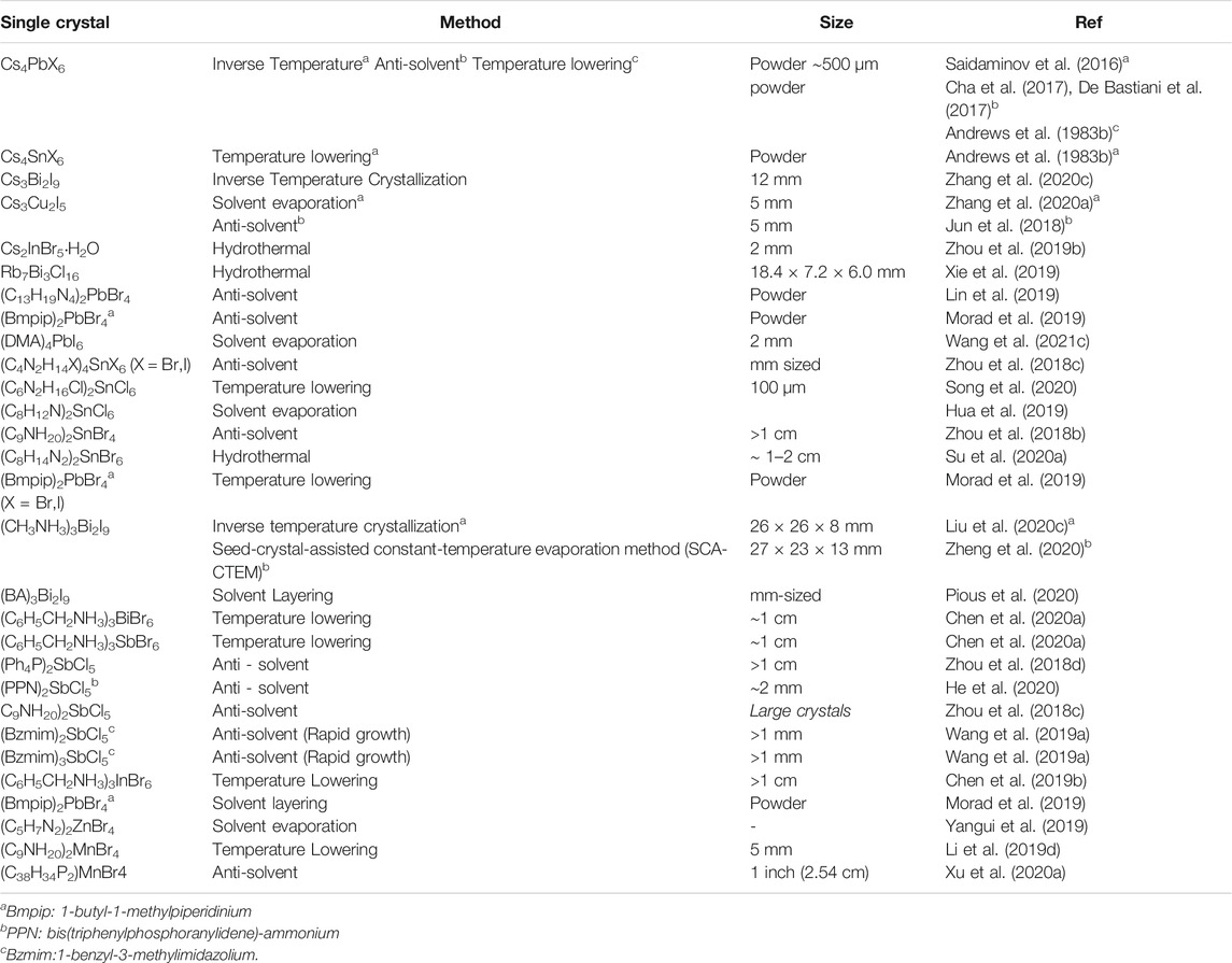
TABLE 2. Summary of 0D single crystals growth by various solution-based methods with their sizes.
Up to this point, 0D HPd crystal growth has mainly been achieved by solution-based growth methods discussed that require numerous types of solvents and might be time-consuming. In recent years, solvent-free synthesis methods such as the Bridgman method and mechanochemical synthesis have received significant attention due to their ease of implementation and solvent-free conditions (Palazon et al., 2019a). Herein, we review solvent-free solid-state techniques used to synthesize molecular 0D HPds.
The Bridgman method is a melt-based technique and widely-used method for growing large crystals as a solvent-free synthesis method (Ding and Yan, 2017). It is a well-known technique for forming various single crystals such as GaAs, ZnSe, CdS used in semiconductor technology (Rudolph and Kiessling, 1988; Razeghi, 2002). The crystallization process occurs inside a quartz ampoule, which is filled with the precursors and sealed under-vacuum. It is then heated above the polycrystalline material’s melting point and moved through a temperature gradient towards the furnace’s colder region. At a specific temperature, the formation of a single crystal begins at the tip of the ampoule and grows along the ampoule’s length. The crystallization can be conducted in a horizontal or vertical geometry. The interface curvature can be adjusted easily by changing the temperature difference of the hot zone and the cold zone of the quartz ampoule. Despite advantages of simple implementation and formation of large single crystals, contact with the ampoule creates mechanical stress and increases the impurity level and defect density (Braescu, 2008). Therefore, a small temperature gradient, slow growth rate, and cooling rate are crucial to avoid crystal cracks and structural defects (Li et al., 2021a). In addition, purification should be carried out before loading the ampoule into the Bridgman furnace. During the sealed ampoule transfer inside the furnace, impurities with different melting points get separated from the crystal. However, if the impurities have similar solubility in the melt as in the crystals, they would not be removed and lead to low-quality single crystals. Thus, purification needs to be done in a separate process before crystal growth (Jiang and Kloc, 2013). For example, purification can be made by drying the mixture under vacuum and baking at elevated temperatures to remove residual impurities (Wu et al., 2018). Another idea is to repeat crystal growth by the Bridgman technique more than once as the impurity level decreases after each repetition time (Dos Santos et al., 2017). Additionally, a pure chalcohalide compound, Tl6SeI4, was obtained with a highly efficient purification method using a bent ampoule to evaporate the main precursors, Se, Tl2Se and TlI and remove the main impurities such as Pb, Bi, Al, Te, Sn and Cl (Lin W. et al., 2018). So far, only purely inorganic single crystal HPs with a specific melt temperature could be synthesized by the Bridgman method.
Hybrid organic-inorganic HP single crystals have not been synthesized by this method since organic compounds have high vapour pressure and are chemically unstable at their melting point (Arya et al., 2020). The well-known zero-dimensional Cs4PbBr6 crystal was synthesized by Nitsch and co-workers in 1995 through the Bridgman method with a precise temperature gradient and translation rate. Before being placed in the vertical Bridgman-Stockbarger furnace, Cs4PbBr6 powder was flame-sealed in a silica tube under vacuum (Nitsch et al., 1995). Recently, several studies were done on inorganic 0D HPd single crystals grown by the vertical Bridgman method on the millimetre scale as summarized in Table 3. Using the vertical Bridgman method, Sun et al. (2018) reported the growth of Cs3Bi2I9 (CBI) single crystals where CsI and BiI3 were reacted in a stoichiometric ratio in a quartz ampoule. The sealed quartz ampoule was then heated to 652 °C (925 K) for 24 h with a temperature gradient (∇T) of 15–20 K cm−1, followed by transferring the ampoule into a two-zone Bridgman furnace for crystal growth. The furnace was then cooled to room temperature at a rate of 4–8 K h−1 and a dull-red large single crystal with a diameter of 15 mm was grown.
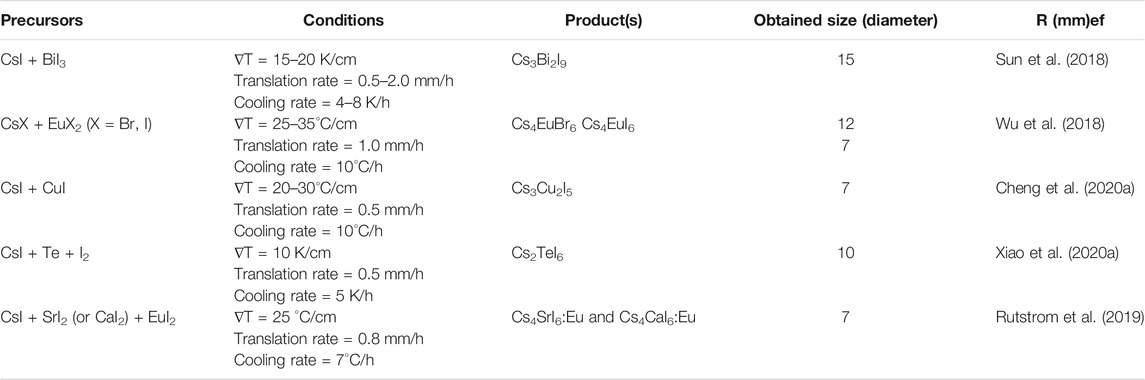
TABLE 3. Summary of 0D HPds grown by the Bridgman method with reaction conditions, temperature gradient (∇T), and obtained crystal diameters.
Similarly, Wu et al. (2018) have grown Cs4EuBr6 and Cs4EuI6 single crystals by employing a solid-state reaction. Mixtures of CsBr (or CsI) and EuBr2(or EuI2) were heated in evacuated quartz ampoules at 250⁰C for 10 h to reduce water and oxygen impurities. After baking, they were sealed and placed into the furnace, passed through a temperature gradient (∇T) of 25–35⁰C cm−1 and subsequently cooled to room temperature at a rate of 10⁰C h−1.12 mm of Cs4EuBr6 and 7 mm of Cs4EuI6 single crystals were obtained. Recently, Cheng S. et al. (2020) reported the growth of Cs3Cu2I5 single crystal by employing the vertical Bridgman method. The ampoule was filled with the reaction mixture of CsI and CuI and sealed under-vacuum. Before growth, the Cs3Cu2I5 compound was synthesized a few degrees above all component’s melting points for 24 h. The growth process started at 390°C with a temperature gradient of 20–30°C cm−1. A Cs3Cu2I5 single crystal with a diameter of 7 mm was obtained with high purity after cooling to room temperature. Similarly, Cs2Tel6 crystals with a diameter of 10 mm were obtained with this method by Xiao et al. During the synthesis of these crystals, they found that raising the temperature over 610⁰C resulted in the ampoule bursting due to the overpressure of iodine. Initially, the overheating temperature was set at 650°C and kept for 24 h, which resulted in the bursting of the ampoule because of the overpressure from iodine. Then, the overheating temperature was reduced to 610°C for 12 h, and a black Cs2TeI6 ingot with dimensions of 10 mm × 55 mm was successfully obtained (Xiao B. et al., 2020). In another study, Eu2+-doped and Cs4SrI6 crystals with sizes of 7 mm were prepared by melt growth, and crack-free crystals could be grown with Eu2+ dopant concentration as high as 9%. (Rutstrom et al., 2019).
Mechanochemical reactions are induced by mechanical energy input by grinding or milling of two or more solid reactants (James et al., 2012). They have many benefits, including great simplicity, economic and environmental friendliness, when compared to other methods (Ben-Akacha et al., 2020). This method may also be advantageous from a thermodynamic perspective as the solid-state reaction’s driving force is more significant than the solution-based one due to the higher chemical potential in solid-state. Furthermore, the different compositions obtained during solution-based synthesis due to the coexistence of different metal complexes in equilibrium are circumvented in solid state methods. Though the particle size is limited, it might be the alternative method for measuring physical properties in the form of pellets discussed in section 2.2. Pal et al. (2018) reported the mechanochemical synthesis of Cs4PbBr6 and Cs4PbCl6 HPs. In this method, Cs-halide (CsCl or CsBr) and Pb(II)-halide (PbCl2 or PbBr2) were mixed in stoichiometric ratios in a mortar pestle then the powder was cold-pressed to make the bar-shaped pellet. They have also performed post-synthetic solid-state transformations of 3D CsPbBr3 to 0D Cs4PbBr6 without using any organic ligand by single step mechanochemical grinding. Pre-synthesized 3D CsPbBr3 were mixed with PbBr2 and CsBr in stoichiometric ratios with a mortar and pestle in N2 environment. In some cases, HP phases are obtained by heating the mixture of reactants at a defined temperature in air or under N2. Benin et al. (2018) performed mechanochemical synthesis under N2 at 350°C for the fabrication of Cs4SnBr6 in the form of pellets and single crystals (20–40-micron diameter). They obtained a mixture of different phases such as CsBr, CsSnBr3, and Cs4SnBr6 upon cooling the melt as it undergoes a peritectic decomposition when heated above 380⁰C. Thus, they concluded that a pure phase synthesis of Cs4SnBr6 could only be obtained by annealing a solid mixture of CsBr and SnBr2. Huang et al. (2020) obtained the Cs3Cu2I5 HP structure by a facile low-temperature solid-state reaction approach. CsI and CuI precursors were ground into a homogenous mixture by using agate mortar. The mixture was poured into alumina crucibles and fired at 350⁰C for 6 h. The crystalline product was collected after the cooling down of the furnace. Although thermal annealing may lead to inhomogeneous phases in the crystalline produce, the proposed method with a well-defined calcination temperature resulted in high phase purity of Cs3Cu2I5 HP material.
In general, ball milling results in cleaner crystalline products than manual grinding due to the possible unreacted precursors left by manual grinding (Stoumpos et al., 2013; Prochowicz et al., 2015). In the ball milling technique, one uses the container and grinding balls made of high-hardness materials such as zirconium, corundum or stainless steel (Protesescu et al., 2018). This method is based on mechanical friction between the balls and ground material; during the container (or bowl) rotation, the mechanical energy transferred from the milling balls to the precursors leads to elastic and plastic deformation dislocations to form a final product. Optimization of container speed, number and size of grinding balls, and the grinding time may help control the size of the crystals (Zhang et al., 2014; Palazon et al., 2019b; Rosales et al., 2019). Cs3Cu2I5 HP has been prepared by dry ball milling method at room temperature (Xie et al., 2020). A steel bowl containing the mixture of the precursors was installed in the ball mill and the final product with a diameter of 0.71 μm was obtained by grinding at 1,000 r min−1 for 30 min. In some instances, a small amount of solvent is included for such reactions since it allows the formation of a paste during grinding and conversion of the mixture into the product in a shorter time (solvent-assisted mechanochemical synthesis) (Bowmaker et al., 2008). Recently, Ben-Akacha et al. (2020) synthesized 0D (Ph4P)2SbCl5 and (Ph4P)2MnCl4 compounds exhibiting similar photophysical properties to single crystals prepared by a mechanochemical synthesis. The 0D HPs were prepared by a solvent-assisted ball milling method where the precursors (SbCl3 and Ph4PCl) and a small amount of diethyl ether were introduced into a stainless-steel container with balls, under N2. The product was obtained after 30 min of grinding with a frequency of 1800 r/min. Diethyl ether was used as a dispersant which improved the milling process. The addition of a small amount of solvent enhanced the reaction rate and resulted in a higher product yield. Wet milling affects the rate of formation of nanocrystals, but it has to be considered that the contamination due to wearing of the container and balls might be higher compared to dry milling (Balaz et al., 2013).
Pelletizing consists of agglomerating powders or nanocrystals by mechanical action to obtain a thick polycrystalline structure. In this section, we will consider pressing methods, with and without an elevated temperature (hot press and cold press, respectively). This synthesis technique is suitable when large samples (laterally and/or in thickness) are required for the application, which could be ferroelectrics, piezoelectrics or thermoelectrics, for example. The sample thickness and diameter can be varied by simply changing the die. The advantage of the manageable dimensions is, however, followed by the difficulty of obtaining compact and monocrystalline compounds. The bulk density is a crucial parameter for defining a good sample, with most applications requiring >95% of the pure crystal density in pellet form. The pellet polycrystallinity can be partially controlled by the particle size of the precursor powders, precursors’ composition, applying a post-press treatment, or using heat during the pressing step.
HPs possess good plasticity, so they can be successfully synthesized by pressing their powders, even in the absence of a polymer binder. Shrestha and collaborators demonstrated that a compact CH3NH3PbI3 pellet could be produced by this method (Shrestha et al., 2017). In this section, we review the pellet press methods (cold and hot press) used to synthesise quasi 0D HPds and highlight the implementations of these methods to obtain good quality pellets.
Cold press was used to fabricate pellets of Cs4SnBr6 and Cs4-xAxSn(Br1-yIy)6 (where A is Rb or K) (Benin et al., 2018). CsBr and SnBr2 were mixed (4.5:1 M ratio), ground in a mortar, and cold pressed with a pressure greater than 5 tons of pressure, in a 13 mm dye. The pellet was then placed in a Pyrex tube under vacuum (10–2 - 10–3 mbar) and kept at 350°C for 60 h. The process was repeated twice to obtain a compact pellet. The materials examined showed strong emission from 500 to 620 nm, coming from trapped excitons, and this was tuneable according to the composition (Benin et al., 2018). Later on, the authors reported the strong temperature dependence of the photoluminescence lifetime in Cs4SnBr6 pellets (Yakunin et al., 2019). They found that the de-trapping process of the localized self-trapped excitons (STEs) has a robust thermal sensitivity. Due to thermally assisted STE de-trapping, the emission is strongly affected by the temperature. Through exciton–phonon coupling, the lattice around a STE can relax to its original state via a fast non-radiative channel. Relaxation times, typically in the range of microseconds to milliseconds, are therefore thermally activated and have recently been employed in lighting-based applications (Yakunin et al., 2019). In 2020, millimetre-thick pellets of the quasi 0D (CH3NH3)3Bi2I9 were reported (Tie et al., 2020). In polycrystalline pellets, reaching a uniform elements distribution could be challenging; the authors tried to ensure a homogenous stoichiometry using powder obtained by grinding single crystals of the target material rather than its precursors (Figure 3A). The (CH3NH3)3Bi2I9 crystals were produced by the solvent evaporation method: the precursors dissolved in GBL were placed in a beaker inside an oven at 70°C for 24 h. The synthesised crystals were rinsed with isopropyl alcohol (IPA) and ground. The resulting powders were then compacted using a compressor. The compound was transferred to a cold isostatic press under a pressure of 0.2 GPa. The pellets were dense, 3.86 g cm−3, comparable to the single crystal density (3.98 g cm−3), with a compact and flat surface. The pellet granules had a size of tens of micrometres, and XRD analysis confirms hexagonal symmetry (P63/mmc). The charge carrier mobility (μ) was evaluated by the time of flight (TOF) method, which gave μ of 1.3–3.3 cm2 V−1 s−1 for the holes and 1.4–3.6 cm2 V−1 s−1 for electrons, therefore showing ambipolar charge transport. Hall effect measurements revealed p-type conductivity (mobility of 2.3 cm2 V−1 s−1), consistent with the TOF analysis (Tie et al., 2020).
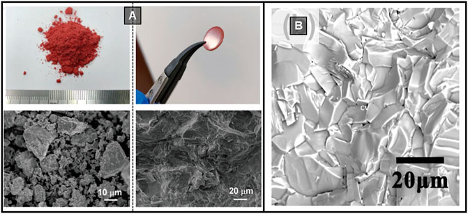
FIGURE 3. (A) (CH3NH3)3Bi2I9 precursor powders and cold-pressed pellet (top) and related SEM images (bottom). Reproduced with permission (Tie et al., 2020). Copyright 2020, Advanced Materials. (B) SEM image of (CH3NH3)3Bi2I9 hot-pressed pellet. Reprinted with permission (Long et al., 2019) Copyright 2019, Applied Physics Letters.
(CH3NH3)3Bi2I9 pellets (Figure 3B) were first produced in 2019 using a hot press method, i.e., a temperature is applied during the pressing process step (Long et al., 2019). The authors choose the method to melt the grains boundaries, increasing the compactness and, consequently, improving the electrical properties. The whole process is performed in a glove box. The powders were obtained by the mechanical alloy method using a high energy ball mill: the precursors were ground in 50 ml jars. The resulting powders were loaded into a graphite dye and pressed at 250°C for 1–2 h, with a pressure of 40 MPa. The pressing was released at 70°C, and the sample allowed to cool naturally. After 30 min of pressing, the tetragonal phase was formed with a relative density greater than 95%. An extraordinarily high Seebeck coefficient of +2.6 mV K−1 and an extremely low thermal conductivity of 0.21 W m−1 K−1 were reported. Scanning electron microscope (SEM) images showed the formation of the cracks along the grain boundaries, which the authors attributed the fragility to the liquid phase formation that happens only at temperatures close to the decomposition temperature of the compound (Long et al., 2019).
In general, thin thin-films are mainly used in nanotechnologies to obtain solids in which the surface properties (e.g., reflection, hardness, permeation, corrosion and electrical behaviour) are enhanced (Frey and Khan, 2015). They can be deposited through various processes, and the method impacts on morphology, microstructure, optical and electrical properties, so the process must be carefully matched to the application. For HPs, the choice of the deposition technique, whether from solution or vapour, determines the crystallization kinetics. Typical HP thin-film thicknesses ranges from 100 nm to 1 μm (Roy et al., 2020). Therefore, the synthesis techniques are modulated according to the thin-film application. In this section, we review the thin-film deposition methods that have been used for the synthesis of 0D HPd. We first analyse the wet deposition (spin coating, multistep methods, drop-casting), then we will move to vapour assisted deposition and electrospray. The primary limit for obtaining a thin film from 0D compounds is related to layer’s compactness and morphology. The management of crystallization kinetics in these HPs is, indeed, quite complex. Many works report the formation of large crystals badly connected, and even in the most optimised methods, the surface roughness remains a challenge to control.
Spin coating is commonly used in many technological sectors to deposit thin films on flat substrates or to deposit sacrificial photoresists as part of a patterning process. The advantage is that very uniform films can be produced in a short time. However, uniform coverage over large areas can be challenging for some materials, and successful deposition is highly dependent on the roughness and surface energy of the substrate to be coated. During the spinning, the solvent evaporates, and the interplay between the centripetal force (coming from angular velocity and acceleration parameters), solvent evaporation rate, and the liquid surface tension will generate a uniform coverage in an optimised process. In producing HP thin films, spin-coating is the most widely used technique because it is simple and low cost. The solvents used to create the ink are generally aprotic polar, with a low vapour pressure at room temperature and a high boiling point. The deposition procedure is usually followed by annealing on a hot plate at temperatures between 70°C and 150°C (Roy et al., 2020).
The first report on spin-coated 0D HPd appeared in 2015 (Figure 4A) (Park et al., 2015a). The materials, bismuth-based HPs ((CH3NH3)3Bi2I9, (CH3NH3)3Bi2I9-xClx, Cs3Bi2I9), were presented as low-toxicity alternatives to lead-based HPs. The HP precursors were dissolved in a DMF/DMSO mixture (7:3 v/v), and the solution was then deposited on a 250 nm thick mesoporous TiO2 layer (1,500 round per minute, RPM. for 20 s) and treated in a dry box (relative humidity below 30%) at 110°C for 30 min on a hot plate. XRD shows that the 0D HPd belonged to the P63/mmc space group and a hexagonal crystalline phase. The absorption spectra recorded for 1 month, storing the samples in the dark and under a dry atmosphere (humidity below 10%), show less than 10% variations, suggesting good stability (Park et al., 2015a). But just a year later, morphology issues became a hot topic. Singh et al. (2016) highlighted how the substrate choice enormously impacted the film morphology (Figure 4B). Deposition on smooth substrates did not generate continuous layers, while in the case of mesoporous layers, nucleation and growth were more uniform. Moreover, they proved that for a good crystallization of a (CH3NH3)3Bi2I9 layer, stoichiometric control (above all the I/Bi ratio) is essential.
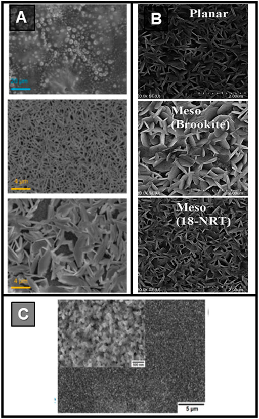
FIGURE 4. (A) SEM images of (CH3NH3)3Bi2I9 (top; scale 20 μm) (CH3NH3)3Bi2I9-xClx (middle; scale 4 μm), Cs3Bi2I9 (bottom; scale 4 μm) thin-films. Reprinted with permission (Park et al., 2015a). Copyright 2015, Advanced Materials. (B) SEM images of (CH3NH3)3Bi2I9 layer deposited on planar TiO2 (top), brookite (middle) and mesoporous TiO2 (bottom); scale 2 μm. Reprinted with permission (Singh et al. (2016). Copyright 2016, ACS Applied Materials & Interfaces. (C) SEM image of (CH3NH3)3Sb2I9 thin-film deposited by a multi-step procedure involving the toluene dripping; scale 1 μm. Reprinted with permission (Hebig et al., 2016). Copyright 2016, ACS Energy Letters.
Abulikemu et al. conducted a comparative study on the crystallization effect on thin films deposited by two procedures: antisolvent-assisted crystallization (ASAC) and saturated vapour crystallization (SVC). ASAC is an anti-solvent procedure in which chlorobenzene (CB) is used; in the SVC procedure, the samples were annealed in a closed Petri dish at 60°C overnight to expose the sample to the solvent vapours (Abulikemu et al., 2016) However, none of the methodologies used provided continuous and compact films, although they reveal that the degree of crystallinity of (CH3NH3)3Bi2I9 heavily affects the optoelectronic properties. Space charge limited current measurements give charge mobility (29.7 cm2 V−1 s−1) comparable to lead HPs, regardless of the substrate. CH3NH3I and BiI3 precursors were dissolved in GBL and a mixture of GBL and DMSO (7:3 v/v). The stable equilibrium between the forming layer and the solvent facilitates the crystallization control. Polycrystalline SVC-produced thin films had an absorption edge at 2.26 eV, compared to the single crystal at 1.96 eV; this shift has already been observed for the 3D HPs CH3NH3PbI3 and CH3NH3PbBr3. The lack of long-range structural coherence, due to disorder in the crystals, usually explains the shift of the optical band gap in thin films (Abulikemu et al., 2016). The authors instead propose that in a 0D HPd, the shift is generated by the electronic transitions in the Bi2I93- clusters. The steady-state optical absorption measurements show a well-defined peak at about 500 nm, very distinct in thin films but not reported in single crystal spectra, probably due to the different crystalline orientation of the thin film; the authors correlated this fingerprint to the electronic transitions in Bi2I93- clusters. Films deposited using GBL solutions have a more pronounced peak and smaller grain size compared to the thin films of the mixture solution. On the other hand, in powders, the optical gap shifts towards greater values, and the colour changes from the intense brown of the crystals to the bright red of the powders. The authors attribute it to the cleavage along the a and b crystallographic plane which generates smaller and more randomly oriented crystallites. The optoelectronic properties of the (CH3NH3)3Bi2I9 thin film were also measured. According to ultraviolet photoelectron spectroscopy (UPS), the work function of the compound, made by the GBL-SVC method, is 4.94 eV and its ionization potential 6.0 eV. The photoluminescence emission band is centred at 637 nm for all samples, suggesting that it should refer to the radiative recombination occurring in Bi2I93- clusters (Abulikemu et al., 2016).
In another method (Öz et al., 2016) CH3NH3I was first dissolved in anhydrous DMF and then BiI3 was added. Spin-coating on PEDOT:PSS takes place after heating the solution to 60°C, and the final annealing was performed at 100°C for 30 min inside a nitrogen-filled glove box. They stated that the Raman peaks in the range 20 cm−1 - 100 cm−1 mainly were assigned to the scissoring I–Bi–I and Bi–I–Bi modes, meanwhile, those ones between 100 cm−1 and 150 cm−1 to the stretching (Bi–I) modes (Öz et al., 2016). Lyu et al. (2016) employed as substrate a fluorine-doped tin oxide (FTO) coated with compact TiO2 and glass: on the first, the roughest surface, the layer was composed of tightly packed hexagons while on glass, a smoother surface, isolated hexagonal crystals are generated. They prepared the precursor solution by mixing BiI3 and CH3NH3I in DMF. After filtration (0.45 µm PTFE syringe filter), the solution was spin-coated then dried on a hot plate at 100°C for 10 min (Lyu et al., 2016).
Another intrinsic feature of 0D HPds is that the strong exciton binding energy becomes a potential limitation for photovoltaic and photodetector devices that require good charge extraction. Scholz and co-authors carried out an in-depth analysis of charge carrier dynamics in (CH3NH3)3Bi2I9 deposited on mesoporous TiO2 (Scholz et al., 2017). In this study, BiI3 and CH3NH3I were dissolved in GBL. The precursor solution was spin-coated onto a mesoporous TiO2 substrate under dry nitrogen in a glove box. In the antisolvent route, 100 μL of CB were dropped after 14 s from the rotation beginning. Drying was done at 70°C for 45 min. An anti-solvent route to film formation was also explored, but this only affected the grain size without altering the charge carrier dynamics (Scholz et al., 2017). In the steady-state absorption spectrum, the excitonic absorption peak at 500 nm (2.48 eV; 20,000 cm−1) is evident. observation of the excitonic peak confirms that in the 0D HPds the charge is confined with typical imprints in the absorption spectrum. Transient absorption (TA) spectra at 400 nm have a triple peak oscillatory structure around 500 nm, which follows the second derivative of the absorption spectrum. Therefore, the authors conclude that many stable excitons are formed following photoexcitation and that local electric fields are present, so substantial as to give rise to a Stark effect. In the band structure, according to density-functional theory (DFT) calculations, two-electron levels, energetically close, are involved, generating two overlapping absorption bands. They suggest, therefore, that the observed phenomena are consistent with a Stark effect induced by trapped carriers (Scholz et al., 2017). The authors state that the I (5p) − Bi(6p) excitation causes the stable exciton formation within the octahedral clusters surrounded by methylammonium. The estimated binding energy is 300 meV, while the average thermal energy at 300 K is 26 meV. Above all, the authors clarify that the excitation kinetics are very different whether it occurs above the band gap or in the exciton band. Only the population with excess energy (λprobe = 465 nm) has an ultrafast decay component, which can be related to the splitting of approximately the 26% of the excitons (Scholz et al., 2017).
In another work, the pronounced localization of excitons is attributed to the packing of (Bi2I9)3− clusters (Ni et al., 2017). In this work, BiI3 and CH3NH3I were mixed in DMF and heated at 60°C under mechanical stirring until the solution was clear. The solution was then spin-coated on silica substrates (2000 RPM), left to rest in air for 30 min, and then annealed on a hot plate at 100°C for 1 h. The absorbance and photoluminescence emission were highly anisotropic. Using the photoluminescence excitation (PLE) technique, the authors observed the absorption transitions between the bands. With excitation at 650 nm, four peaks (385 nm, 464 nm, 557 nm, 615 nm) were detected. The peak intensities are modulated by the incidence angle of the excitation beam, and the PLE spectra for different excitation wavelengths indicate the presence of localized excitons. When the beam is perpendicular to the sample (θ = 0°), the authors pump at excitation wavelengths close to the PLE peaks (λex = 375 nm or 450 nm) and probe in the 580–660 nm range. Excitation at 375 nm gives 3 PL day components (τ1 < 1 ps; τ2 = 10 ps; τ3 > 2 ns), while at 450 nm there are only 2 (τ1 < 1 ps; τ2 > 12 ns). The excitons at 375 and 450 nm were located in the clusters of Bi2I93- and come from states trapped in two different sites. Due to the nanosecond duration of some excitons, it is suggested that a small portion of them is capable of tunnelling through the CH3NH3+ matrix, becoming delocalized. Given the presence of such long-lived delocalized excitons, the possibility of carrier multiplication is predicted. By probing with a different beam wavelength, between 250 and 400 nm, the authors also highlight a group of parasitic peaks related to cascade excitations, indicating that reabsorption and re-emission of photons is possible (Ni et al., 2017).
Other well-investigated compounds are the Sb-based 0D HPds. Baranwal and collaborators (Baranwal et al., 2017), synthesized HPs thin-films based on Sb and Bi, studying them as the cations vary (CH3NH3+, Ag+ and Cu+). The CH3NH3I-based solutions were prepared by dissolving the precursors in a mixture of DMSO and GBL, while the precursors for the solutions with metal cations were dissolved in DMSO. All the solutions were heated at 80°C and deposited at 2000 RPM for 30 s in an inert atmosphere. Then the layers were placed on a hot plate at 80°C for 30 min. The (CH3NH3)3Bi2I9, (CH3NH3)3Sb2I9 and (CH3NH3)3SbBiI9 films all belong to the hexagonal space group P63/mmc and share the same preferential crystal orientation. In the ultraviolet–visible (UV-vis) spectra of (CH3NH3)3Bi2I9 and (CH3NH3)3SbBiI9, a peak appears around 500 nm. In the (CH3NH3)3Sb2I9 spectrum, there is instead a broader feature around 460 nm, but no clear peak. The coating of the substrates used, TiO2 and NiO, is not complete: the surface morphology is composed of interconnected hexagonal crystals. Furthermore, energy-dispersive X-ray (EDX) analysis revealed that the ratio [I/(Sb + Bi)] is not homogeneous. The coverage of TiO2 and NiO substrates is improved compared with the films made with organic cations, even if it is not yet complete and the distribution of the elements remains uneven (Baranwal et al., 2017).
The bandgap of (CH3NH3)3(Sb1-xBix)2I9 can be modulated by varying the Sb/Bi ratio (Chatterjee et al., 2020). In this work, BiI3, SbI3 and CH3NH3I were dissolved in DMF, and the solution stirred at 70°C overnight. Subsequently, it was spin-coated at 2500 RPM for 30 s; after 12 s, 100 µL of CB at 70°C was dropped onto the spinning substrate. Finally, the sample was annealed at 100°C for 30 min. The minimum energy gap obtained was 1.90 eV when the two metals were in an equimolar ratio. This value is significantly lower than the band gap of pristine compounds, which is 2.36 eV for (CH3NH3)3Sb2I9 and 2.16 eV for (CH3NH3)3Bi2I9. The authors explain the phenomenon suggesting antagonism between the lattice deformation and the spin-orbit coupling (Chatterjee et al., 2020). Another work (Hebig et al., 2016) obtained good thin film coverage of pristine (CH3NH3)3Sb2I9 (Figure 4C). No excitonic peaks are clearly visible in the absorption spectrum: the authors attribute this to the substitution of Bi with Sb, but it should be noted that the layers analysed were amorphous. SbI3 and CH3NH3I were dissolved in a mixture of GBL: DMSO (2:3; v/v), and two spin-coating procedures were adopted. In the first, the solution was spin-coated at 3000 RPM for 45 s, while in the second, a multi-step procedure was implemented, where the spin rate was 3000 RPM for 10 s, then increased to 5000 RPM for 35 s, and finally, in the last 20 s, toluene was dripped onto the spinning film. Using the first deposition route, the resulting layer was composed of hexagonal crystallites with non-continuous coverage. On the other hand, the second deposition procedure, involving the toluene dripping onto the film during spin-coating, generated a uniform thin-film whose structure was confirmed by XRD with a strong orientation of the c axis out-of-plane. Compared to Bi-based HPs, (CH3NH3)3Sb2I9 exhibits lower sub-bandgap absorption, indicating a lower defect density. The PL emission peaks at 1.58 eV and the Urbach tail energy at 62 meV, indicate that a substantial amount of disorder is present. A high energetic disorder implies additional tail states that can give rise to non-radiative recombination processes. Furthermore, it is noted that the PL signal is shifted by 560 meV at energies lower than the band gap (2.14 eV), indicating that the luminescence comes from radiative recombination in sub gap states. They attributed the PL peak at 2.05 eV to direct band to band recombination (Hebig et al., 2016).
Excitonic peaks were instead reported in (CH3NH3)3Sb2I9 by Scholz and collaborators in polycrystalline thin films (Scholz et al., 2018). They dissolved SbI3 and CH3NH3I in different solvents: GBL, in a mixture of GBL and DMSO (3: 2 or 2: 3 v/v) or DMF. A two-step procedure was performed in the glovebox: first, the substrates were spin-coated at 500 RPM, then at 3000 RPM for 30 s. CB was dripped onto the films after 4 s for the GBL/DMSO solutions, after 6 s for those in DMF and after 14 s for GBL. The samples were then placed on a hot plate for 30 min at 80°C (GBL and DMF) and 110°C (GBL/DMSO). The films were not continuous, but transient UV-vis-near-infrared (UV-vis-NIR) femtosecond absorption spectra show marked excitonic characteristics. The time scales of the different scattering processes were analysed, finding that the kinetics (recombination time constants, τ1 = 190 ps, τ2 = 5 ns) were pump laser fluence independent, meaning the dynamics could involve localized excitons. Non-radiative recombination mechanisms dominate the exciton dynamics. The phononic dynamics were coherent, showing a strong electron-phonon coupling. Steady-state Raman spectra were dominated by the vibrations of (Sb2I9)3− anions. In the steady-state spectra, the shoulder around 470 nm is assigned to exciton absorption, with a binding energy >200 meV. The second derivative of the steady-state absorption spectrum is very similar to the 10 ps broadband transient absorption spectra. The authors attribute this spectral signature to the predominant presence of excitons, which can be generated either by a Stark effect induced by a trapped carrier or by a biexciton effect. The observed kinetic behaviour is consistent with locally trapped excitons, recombining non-radiatively over long time scales. This interpretation is in agreement with a strong electron-phonon coupling, that is confirmed by the strong oscillations observed in the kinetics (Scholz et al., 2018).
A possible way to increase the electrical conductivity is represented by doping. Electrical doping to increase charge carrier concentration has been used in 3D HPs (Liu et al., 2019; Tang et al., 2020; Euvrard et al., 2021b), but remains relatively unexplored in 0D HPds. Vigneshwaran et al. (2016) engineered the (CH3NH3)3Bi2I9 bandgap by doping it with sulphur. They obtained a mixed HP with a band gap of 1.45 eV, where the charge carrier concentration and mobility have been increased compared to the pristine material. The precursor solution was prepared by mixing Bi(xt)3 (xt = ethyl xanthate) and CH3NH3I (molar ratio 1: 2) in DMF. The filtered solution was spin-coated on mesoporous TiO2 (2000 RPM for 15 s). Different annealing temperatures were tested: 80°C, 120°C and 150°C. The final morphology of their (CH3NH3)3Bi2I9 layers was investigated through SEM analysis, and image of the sample annealed at 120°C is shown in Figure 5A. The thermal decomposition of the metal xanthates eventually leads to the formation of Bi2S3, through the formation of volatile intermediates such as CS2, COS, CO2 and CO. When decomposition occurs in the presence of CH3NH3I, (CH3NH3)3Bi2I9 formation is favoured, with X-ray photoelectron spectroscopy (XPS) analysis confirming sulphur doping. The band gap was reduced by increasing the annealing temperature. Fourier-transform infrared (FTIR) spectroscopy and thermogravimetry/differential thermal analysis (TG-DTA) show that the minimum post-heating temperature to remove impurities and complete the doping is 120°C. Hall effect measurements showed p-type semiconductor behaviour with carrier mobility of 2.28 cm2 V−1 s−1, and annealed samples had a carrier concentration of 2.3 × 1021 cm−3, which is five orders of magnitude higher than the undoped (CH3NH3)3Bi2I9 (Vigneshwaran et al., 2016).
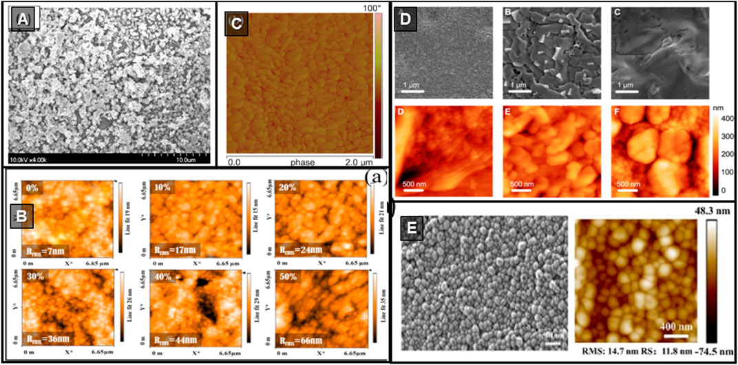
FIGURE 5. (A) Sulphur-doped (CH3NH3)3Bi2I9 annealed at 120°C; scale 10 μm. Reprinted with permission (Vigneshwaran et al. (2016)). Copyright 2016, Chemistry of Materials. (B) AFM surface topography of Sn4+-doped (CH3NH3)3Sb2I9 layers, varying the tin percentage. Reprinted with permission (Chatterjee and Pal, 2018). Copyright 2018, ACS Applied Materials & Interfaces. (C) AFM surface topography of pin-holes free (NH4)3Sb2I9 thin-film. Reprinted with permission (Zuo and Ding, 2017). Copyright 2017, Angewandte Chemie International Edition. (D) SEM images and AFM surface topographies of Cs3Sb2I9 (left), Rb3Sb2I9 (centre), K3Sb2I9 (right). Reprinted with permission (Correa-Baena et al., 2018). Copyright 2018, Chemistry of Materials. (E) SEM image and AFM surface topography of Cs3Cu2I5. Reprinted with permission (Zeng et al., 2021). Copyright 2021, The Journal of Physical Chemistry Letters.
Bismuth HPs with mixed halides were synthesized to study the change in crystal structure. Hoefler and co-workers (Hoefler et al., 2018), partially substituted iodine with chlorine in (CH3NH3)3Bi2I9. The incorporation of chloride changed the crystal structure, moving it to pseudo-stratified 0D (Hoefler et al., 2018).
In another work, (CH3NH3)3Sb2I9 was doped with Sn4+ (Chatterjee and Pal, 2018). The Fermi energy moved towards the conduction band with the increase of the tin content, changing the type of conductivity from the p-type to the n-type. However, the tin substitution degraded the surface morphology, as shown by atomic force microscopy (AFM) images in Figure 5B, so the authors varied the Sb/Sn ratio to obtain the maximum reduction of the band gap and the lowest surface roughness. CH3NH3I, SbI3, and SnI4 were dissolved in stoichiometric quantities in anhydrous DMF, and the solution left at 70°C overnight. One drop of the solution was spin-coated at 2500 RPM for 30 s; at 12 s, 100 μL of CB at 70°C was dropped onto the sample to accelerate the crystallization. Finally, the films were annealed on a hot plate at 100°C for 30 min. Following the tin substitution, the spectral absorption region shifts to longer wavelengths. The Tauc plot reveals that the optical gap decreased by 0.1 eV for every 10% of Sn4+. Generally, doping in semiconductors leads to the Burstein-Moss effect, which consists of apparent widening of the optical band gap due to the occupation of states at the band edges by free charge carriers. However, an opposite behaviour in the 0D HPds has been recorded. The authors attributed this effect to the introduction of impurity levels into the band gap: the width and number of those levels increases as Sn4+ is added, reducing the effective band gap (Chatterjee and Pal, 2018). XRD shows that the preferential orientation is with the c axis out-of-plane. In samples containing more than 10% Sn4+, an additional peak at about 12.7° appears, which is attributed to the (111) plane of the secondary phase (CH3NH3)2SnI6, a low-order 0D structure. The valence and conduction bands were determined by scanning tunnelling spectroscopy (STS). It is noted that the binding energy of the exciton decreases as the doping increases, reducing from 200 to 110 meV in the case of 50% tin replacement; therefore, the transport gap is reduced in tandem with the optical gap. The data show that the gap reduction is due to the modulation of the conduction band alone. The STS analysis also showed that the Fermi level shifts towards the CB as the tin content increases. Therefore, the conductivity changes from type p to type n (confirmed by Hall effect measurements). However, it was also observed that the surface roughness increases with dopant concentration. A good compromise between band gap reduction and surface roughness was found at 40% Sn doping (Chatterjee and Pal, 2018).
A novel compound (NH4)3Sb2I9 can produce pin-holes free thin-film, with the roughness of 5.5 nm and grains of 40–200 nm (Figure 5C) (Zuo and Ding, 2017). These can be prepared by mixing the precursors (NH4I and SbI3; NH4Br and SbBr3) in ethanol. The layers were made on poly (3,4-ethylenedioxythiophene) polystyrene sulfonate (PEDOT:PSS) by spin coating at 4000 RPM for 30 s. Then the samples were annealed on a hot plate at 110°C for 2 min. The absorption spectrum of (NH4)3Sb2I9 could be gradually modulated by replacing I with Br. Analysis of the Tauc plot shows that (NH4)3Sb2I9, (NH4)3Sb2I6Br3, (NH4)3Sb2I3Br6 and (NH4)3Sb2Br9 films have direct optical gaps of 2.27, 2.49, 2.66 and 2.78 eV, respectively. The XRD diffraction peaks show a strong orientation of the c-axis out-of-plane, suggesting high crystallinity (Zuo and Ding, 2017).
Sb-based HPs can also be synthesised when changing the A-site cations (where A is Cs, Rb, or K) (Correa-Baena et al., 2018) (Figure 5D). In this case, SbI3 was dissolved in a mixture of DMF and DMSO (9:1 v/v) and heated at 100°C for 15 min. CsI was dissolved in DMSO, while RbI and KI in a mixture of DMF and DMSO (9:1 v/v). The solutions were spin-coated in the glovebox in two phases, the first at 1000 RPM for 10 s, the second at 5000 RPM for 20 s. During the second phase (after 5 s), CB was dripped onto the substrate; then, the film was annealed on a hot plate at 100°C for 20 min. As expected, the cation exchange affects the band gap, which ranges from 2.02 to 2.43 eV. The XRD pattern of the thin films based on Cs, Rb and K show a high preferential orientation of the (003) direction out-of-plane. Then the authors analysed the powders, concluding that Cs3Sb2I9 crystallizes in the space group P63/mmc (0D), while K3Sb2I9 and Rb3Sb2I9 form 2D structures. Cs3Sb2I9 showed an excitonic peak at 570 nm. The steady-state PL shows sharp emission at 774 nm, suggested to be related to a trap-assisted emission. The time-resolved photoluminescence (TRPL) decays were composed of initial fast bleaching, followed by a slower one: they were slower in the 0D structure than in the 2D compounds due to the high exciton binding energy (166 meV for the 0D HPds based on Cs; 107 and 120 meV, for the 2D HPs based on Rb and K, respectively) (Correa-Baena et al., 2018). These results are debated: Correa-Baena et al. derived the above exciton binding energy values based on the default assumption that the observed PL is associated with free exciton recombination. However, other investigations of the PL emission of these materials demonstrates that the observed PL is associated with the recombination of self-trapped excitons, hence the thermal quenching of the PL cannot be traced to the exciton binding energy (McCall et al., 2017; Mei et al., 2021.). It has to be mentioned that zero-dimensional Cs3Sb2I9 features considerably stronger exciton self-trapping than the two-dimensional counterparts, reflecting the more prominent trapping effects taking place with lower structural dimensionality (Mei et al., 2021).The cation substitution impacts the films morphology: the Cs3Sb2I9 film comprised small grains, while those of Rb3Sb2I9 and K3Sb2I9 displayed much larger grains (Correa-Baena et al., 2018).
Cs3Sb2I9 has two polymorphs, one with a 2D structure and the other 0D, which can be selected according to the deposition procedure (Singh et al., 2018). The precursor solution was obtained by dissolving SbI3 and CsI in a mixture of DMSO and DMF (3:1 v/v), and then kept under continuous stirring at 70°C for one night. It was spin-coated on PEDOT:PSS-coated substrates at 6000 RPM for 40 s. Then, the samples were placed on a hot plate at 150°C to obtain the 0D structure and at 70°C for the 2D. The 2D HP films were, then, placed in a bottle containing SbI3 (drops of a solution in DMF), and the system was heated to 250°C to complete the structure formation. The absorption spectra of both structures have three different absorption peaks. The authors suggest that they arise from transitions in the same band. The band gaps were direct, evaluated as 2.3 eV for the 0D structure and 2.05 eV for the 2D (Singh et al., 2018).
It has been proven that the carrier mobility of 0D Cs3Sb2I9 is considerably lower than the 2D counterparts: the 0D and 2D carrier mobility, estimated using the space charge limit current (SCLC) method, are reported to be 3.54 cm2 V−1 s−1 for the 0D phase and 6.81 cm2 V−1 s−1 for the 2D, suggesting that the layered structure has a lower defect concentration (Umar et al., 2019). Also Peng and collaborators were able to improve the charge mobility by tuning the structure (Peng et al., 2020), substituting some of the iodine in Cs3Sb2I9 with chlorine. They found that the average Hall mobility of the 2D compound (Cs3Sb2Cl3I6) was 5.7 cm2 V−1 s−1, meanwhile for Cs3Sb2I9 in the 0D phase was 0.5 cm2 V−1 s−1 (Peng et al., 2020).
Recently, the inorganic HP, Cs3Cu2I5, has been deposited on an indium tin oxide (ITO) substrate inside a glovebox (Zeng et al., 2021). The precursor solution was spin-coated at 1000 RPM for 10 s before and at 4000 RPM for another 20 s 100 µL of methyl acetate were dropped as anti-solvent at the end of the spin process. Then, the film was placed on a hot plate at 100°C for 1 h. Different HI amounts (0, 5 and 10 μL) were added to promote the crystallization of the film. XRD analysis attributes the material to the orthorhombic space group Pnma. HI affects the peaks intensity, allowing the authors to conclude that the best crystallinity is obtained by adding 5 μL of HI. All the films were uniform, with the size of the grains decreasing as the amount of added HI increases. The surface roughness was generally less than 20 nm, and the lowest value, 13.3 nm, is obtained by adding 5 μL of HI (Figure 5E). Cracks are seen only in the film with 10 μL of HI. The authors conclude that adding a moderate amount of HI can improve crystallinity and morphology, but an excess of it can be detrimental due to the water introduced in the precursor solution by the HI (Zeng et al., 2021).
The literature indicates that Sb-based 0D HPds have better film-forming properties and lower exciton binding energy than those based on Bi. This points to some potential benefits of employing antimony instead of bismuth when replacing Pb in thin film applications.
To produce uniform (CH3NH3)3Bi2I9 films, some groups have designed multistep depositions, in which BiI3 is deposited first and, subsequently, CH3NH3I is provided in various ways to complete the synthesis. Wang et al. (2017) spin-coated the BiI3 solution and, soon after, a CH3NH3I drop placed on the surface then the excess spun-off. The synthesis was completed by annealing on a hot plate. BiI3 had been dissolved in DMF, sonicated for 30 min, and then filtered. The deposition was performed in a glove box in a two-step procedure (2000 RPM for 5 s and 5000 RPM for 10 s). Then the sample was placed on a hot plate at 100°C for 30 min. Soon after, 100 μL of CH3NH3I in IPA (3 mg ml−1, 6 mg ml−1; 10 mg ml−1; and 20 mg ml−1), was spread on the BiI3 film and left to rest for 30 s, then spin-coated at 4000 RPM for 20 s. Finally, the sample was annealed at 100°C for 60 min. All the synthesis was performed in the glovebox. For comparison, a one-step method was also implemented: the (CH3NH3)3Bi2I9 solution was obtained by mixing the precursors in DMF, sonicated for 30 min, and filtered. 35 μL were deposited and spin-coated at 4000 RPM for 30 s, and the sample placed on a hot plate at 100°C for 30 min. The two-step methodology offered better coverage than the one-step method (Figure 6A). Furthermore, the authors highlighted that the film morphology was strongly correlated to the concentration of the CH3NH3I solution. The best compromise between substrate coverage surface and roughness was found to be 6 mg ml−1 (Wang et al., 2017).
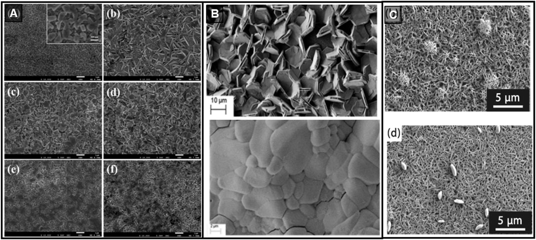
FIGURE 6. (A) SEM images of BiI3 (top-left), one-step solution (CH3NH3)3Bi2I9 (top-right), and two-step (CH3NH3)3Bi2I9 prepared with various concentration of CH3NH3I: 3 mg ml−1 (centre-left), 6 mg ml−1 (centre-right), 10 mg ml−1 (bottom-left), and 20 mg ml−1 (bottom-right). Reprinted with permission (Wang et al., 2017). Copyright 2017, RSC Advances. (B) SEM images of (CH3NH3)3Bi2I9 deposited by single-phase deposition (top) and multistep method. Reprinted with permission (Ahmad et al., 2019). Copyright 2019, ChemElectroChem. (C) SEM images of (CH3NH3)3Bi2I9 deposited by Hot Air Blow-Assisted Spin-Coating method and annealed at 130°C (top) and 150°C (bottom). Reprinted with permission (Shirahata, 2020). Copyright 2020, Journal of the Ceramic Society of Japan.
The organic cation can instead be introduced through an organic solution of metal salts (Chen M. et al., 2018). In this case, the BiI3 was dissolved in DMF, and the solution sonicated and filtered. 15 μL were dripped onto the substrate; then, spin coated at 3,000 rpm for 6 s, followed by 6,000 rpm for 10 s. The samples were placed on a hot plate at 100°C for 10 min in a protected atmosphere, after resting in air for 30 min. The sample was then immersed in a CH3NH3I bath in anhydrous IPA and annealed at 100°C for 30 min. However, the resulting layer was discontinuous, made of hexagonal crystals with a random orientation (Chen M. et al., 2018). Recently, Ahmad and collaborators designed a two-step deposition to obtain a thin film with a compact and smooth surface (Figure 6B) (Ahmad et al., 2019). First, they deposited the BiI3 dissolved in DMF (5000 RPM for 30 s) on mesoporous TiO2 and annealed it at 70°C for 10 min CH3NH3I in 2-propanol was dropped onto the film and spin-coated (2000 RPM for 30 s); then, the film was annealed on a hot plate at 120°C for 20 min. For comparison, they prepared a precursor ink in DMF, and spin-coated it at 5000 RPM for 30 s. The film made by the single-phase deposition had a very rough hexagonal flake morphology (7.57 μm grain size). Instead, the film prepared by the multistep method had a much more compact surface, made up of large grains (size 17.25 μm). The films show the typical absorption features, and the calculated optical band gap was 2.2 eV. XRD analysis indicated remarkable stability up to 2 months (Ahmad et al., 2019).
A Hot Air Blow-Assisted Spin-Coating method was introduced recently to deposit (CH3NH3)3Bi2I9 (Shirahata, 2020). SEM images are displayed in Figure 6C. The precursor solution was deposited on mesoporous TiO2 and spin-coated at 2000 RPM for 30 s, without hot air blowing. Then, the deposition was repeated with the substrate at 60°C and with blowing. Finally, the samples were placed on a hot plate at temperatures between 120 and 150°C for 30 min. The surface morphology, the I/Bi ratio, and the lattice constants were dependent on the annealing temperature. The best sample was obtained with annealing at 130°C (Shirahata, 2020). Hence, the subsequent spin coating of the two precursors appears to be a winning method to produce good quality and continuous (CH3NH3)3Bi2I9 thin films.
Drop casting is a simple deposition method, where a precursor solution is spread and dried by controlling temperature and pressure. The final thickness depends on the volume of the dispersed solution and its concentration. The thin-film structure is defined by the substrate wettability, the solvent evaporation rate, and the capillary forces associated with drying. A disadvantage of this method is that uniform thin films can only be produced on relatively small substrates (in the order of a few cm2). Pious et al. (2017) used this method to produce (CH3NH3)3Bi2I9 film with a suitable substrate coverage. BiI3 and CH3NH3I were dissolved in DMF and continuously stirred at 70°C overnight. Then the precursor solution was poured into a Petri dish and heated to 100°C for 4 h to evaporate the solvent completely. The produced powders were mixed with PTFE and activated carbon in a weight ratio of 85:10:5. Then the compound was dispersed in ethanol, and it was homogenized by sonication. The ink was dripped onto the substrate, followed by drying at 60°C for 12 h in a vacuum oven. The film comprised interconnected crystals, and the XRD suggested that the material is highly crystalline (Pious et al., 2017). Although the deposition process is barely used to synthesize 0D HPd, the reported results seem encouraging. The limitation comes from the difficulty to control the drying process to obtain films of suitable thickness and uniformity for many applications.
Vapour deposition covers techniques where materials are transported to a substrate in the vapour phases on which they condense or undergo a chemical reaction. The techniques include chemical vapour deposition (CVD) and physical vapour deposition methods (PVD). As CVD uses a chemical reaction on or near the substrate to form the thin film, it is typically performed at a high temperature. It is highly scalable and includes a number of variants on the core technique, including aerosol-assisted CVD (Ratnasingham et al., 2021), atomic layer deposition (ALD) (Seo et al., 2019), low-pressure CVD (LPCVD) (Luo et al., 2015), plasma enhanced CVD (PECVD) (Qiu et al., 2019), and others. PVD includes a range of techniques such as thermal evaporation (Liu et al., 2019), sputtering, e-beam PVD and pulsed laser deposition. In the 0D HPd literature, vapour deposition has been used both to provide just the organic salt, or to deposit all the precursors sequentially or in parallel.
Hoye et al. (2016) compared (CH3NH3)3Bi2I9 thin films synthesised by solution processing and vapour-assisted techniques on borosilicate glass and quartz substrates. In the solution-assisted conversion, they first prepared the BiI3 solution in DMF, sonicated for 1 h and filtered. 10 μL was spread on the substrate (spin-coated first at 3000 RPM for 5 s and then 6000 RPM for 5 s) in a nitrogen-filled glovebox. The BiI3 film was left to rest for 30 min and then placed on a hot plate at 100°C for 30 min CH3NH3I was dissolved in anhydrous IPA, and 200 μL of the solution was deposited on the BiI3 film and allowed to rest for 60 s before spinning (4000 RPM for 20 s). In the vapour assisted conversion, the substrates were heated to 150°C for 15 min, 20 μL of the BiI3 solution were dropped onto the substrate and spin-coated at 4000 RPM for 10 s. Then the film was placed on a hot plate at 100°C. The conversion of the metal halide to a 0D HPd was achieved by suspending the film in a vacuum chamber above some CH3NH3I powder which was heated to 150°C for 4 h. After naturally cooling the system to room temperature, the film was annealed at 100°C for 1 h in a nitrogen-filled glove box. The largest crystallites were obtained with the vapour-assisted conversion method, even though the layer is composed of tightly packed flat crystals resulting in a rough, non-continuous thin film (Figure 7A). Transient PL analysis shows that films made by vapour assisted process have longer decay times and therefore lower rates of non-radiative recombination which you would expect from a material with low defect density (Hoye et al., 2016). Ran et al. (2017) managed to create a smooth and compact layer with low surface roughness. First, the BiI3 layer was thermally evaporated under a vacuum of 10–5 mbar, then CH3NH3I solution in IPA was coated by spinning at 4000 RPM for 30 s, and the film annealed at 120°C for 1–5 h. IPA in excess was dripped onto the sample and spin-coated to remove the residual CH3NH3I. BiI3 had a preferential orientation of the (006) parallel to the substrate, and (CH3NH3)3Bi2I9 exhibits the typical peaks of the hexagonal space group P63/mmc. In the UV-vis spectrum, absorption peaks at 2.47 eV, at 2.95 and 3.58 eV are observed that relate to the electron transitions from the ground state 1S0 to the excited states 3P1, 3P2 and 1P1 of Bi3+ in the isolated Bi2I93− clusters. The calculated diffusion lengths for electron and hole are 46.0 and 21.6 nm, respectively. Furthermore, the trap density of the charge carriers was assessed as 5.29 × 1017 cm−3 and their mobility 3.47 × 10⁻⁷ cm2 V−1 s−1. (Ran et al., 2017). A vapour-assisted solution process was also used by Jain et al. (2018) where BiI3 was dissolved in DMF:DMSO (6:4 v/v), and the solution was spin-coated at 4000 RPM. The sample was placed on a hot plate at 100°C for 30 min. The samples were then placed in a closed Petri dish containing CH3NH3I powder and heated to 150°C. The critical step to produce compact films is the reaction time between the BiI3 film and the methylamine in the gaseous phase. The grain size increased with the exposure time to the CH3NH3I vapours. In the UV-Vis spectra, a peak at 495–516 nm appears as the reaction time increases, which is attributed to the exciton peak. This peak has a shoulder at 625 nm, decreasing with increasing reaction time, suggesting that two bands are involved in the electronic transition (Jain et al., 2018). Also, Huang and collaborators applied the sequential deposition method to obtain uniform layers of (CH3NH3)3Bi2I9: first, the BiI3 was evaporated on ITO and immediately after the CH3NH3I; then, the sample was heated at 100°C for 30 min in a nitrogen atmosphere. By varying the deposition ratios of the two precursors, the authors obtained an excellent coverage of the substrate (Huang et al., 2018).
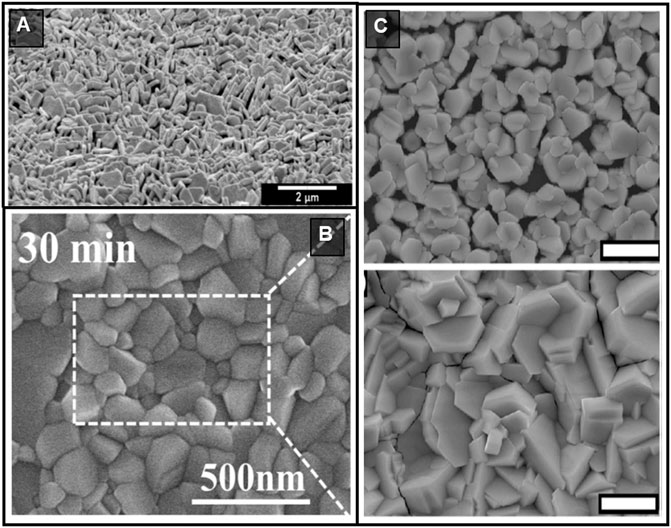
FIGURE 7. (A) SEM image of vapour assisted synthesized (CH3NH3)3Bi2I9 layer (scale 2 μm). Reprinted with permission (Hoye et al., 2016). Copyright 2016, Chemistry–A European Journal. (B) SEM image of S-doped (CH3NH3)3Bi2I9 grown by low-pressure vapour-assisted solution process (scale 500 nm). Reprinted with permission (Li et al., 2019b). Copyright 2019, ACS Energy Letters. (C) SEM image of (CH3NH3)3Bi2I9 thin-films grown by the precursors co-evaporation: deposited for 360 min once (top) and twice (bottom); scale bar 2 μm. Reprinted with permission (Chen et al., 2017). Copyright 2017, Royal Society of Chemistry.
A novel and successful synthesis path to obtain compact and uniform (CH3NH3)3Bi2I9 thin-films has been proposed by Li and co-workers (Li F. et al., 2019). They used vapour deposition to perform organic cation exchange, transforming (CH3CH2CH2NH3)3Bi2I9 to (CH3NH3)3Bi2I9 when it was exposed to CH3NH3I gas. The precursor film was made by spin-coating a solution of BiI3 and CH3CH2CH2NH3I in DMSO. The cation exchange was carried out in methylamine gas, generated by the reaction of methylammonium chloride and sodium hydroxide (CaO was used as a desiccant). The reaction was carried out in a closed container at 100°C for 5 min. The (CH3CH2CH2NH3)3Bi2I9 thin-film has a dense and uniform morphology with grain sizes between 300 and 1,000 nm. Therefore, CH3CH2CH2NH3I assists the reaction and creates large well interconnected grains, and after conversion the layer compactness is kept although the grain size is reduced to about 100 nm (Li F. et al., 2019). A low-pressure vapour-assisted solution process was also developed to grow bismuth-based HP films with iodine partially substituted by sulphur (Li et al., 2019b). The Bi(xt)3 precursor solution in DMF was spin-coated on mesoporous TiO2 at 3000 RPM for 30 s; then, the sample was heated to 70°C for 30 min in a nitrogen-filled glove box. The Bi(xt)3 layers covered with CH3NH3I powder were closed in a Petri dish and placed in an oven under vacuum (10 kPa) at 150°C. After 30 min, the film had become dense and uniform (Figure 7B); the absorption edge was at 743 nm (1.67 eV). By increasing the reaction time, the absorption edge was blue-shifted. The bandgap increased to 2.10 eV when the samples were annealed for 90 min, because prolonged exposure to CH3NH3I vapours causes an excessive substitution of S2- with I−, bringing the structure closer to that of the pristine compound (Li et al., 2019b).
A deposition process involving the gas phase of both the precursors was designed by Zhang et al. to obtain highly compact films with large grains (Zhang Z. et al., 2017) first BiI3 was deposited in high vacuum, then (CH3NH3)3Bi2I9 was synthesised in CH3NH3I gas in low vacuum. The reaction between BiI3 and CH3NH3I takes place in a closed ceramic vessel (reaction space of 3,600 cm3) in a low vacuum oven at 140°C–180°C for 6–10 h. Final annealing in air was applied to remove residual CH3NH3I. The optical bandgap, with a direct transition, is 2.26 eV. The excitonic absorption peak is visible at 498 nm. The spectrum of PL shows four signals: 488 nm (2.53 eV, linked to the energy absorption edge at 2.62 eV), 519 nm (2.39 eV, relative to the exciton PL peak of absorption at 2.62 eV), 575 nm (2.15 eV, consistent with the optical bandgap) and 603 nm (2.05 eV, attributed to the excitonic irradiative luminescence at the band edge) (Zhang Z. et al., 2017).
Co-evaporation of precursors has been widely used for 3D HP films as it can lead to a high-quality film (Liu et al., 2019; Li et al., 2020; Roß et al., 2020). In the context of 0D HPds this method has shown good coverage but with a high roughness (Figure 7C) (Chen et al., 2017). The thin films produced had an indirect optical bandgap of 1.80 eV and an excitonic peak at 511 nm. In contrast to other published reports, the films exhibit the characteristics of n-type semiconductors. The conductivity of a 775 nm film shows a rather high value of 9.7 S cm−1. Moreover, the concentration of the charge carriers was 3.36 1018 cm−3 with a mobility of 18 cm2 V−1 s−1. Through thermogravimetric analysis and the precise positioning of the sources in the reactor, the authors could co-sublime the precursors. CH3NH3I and BiI3 are co-sublimed at 199°C and 230°C, respectively, in argon flow inside a tubular oven. The substrate (silicon or glass) was kept at a temperature of 160°C. BiI3 quickly condensed on the substrate, where it nucleated and grew. The condensation of CH3NH3I determines the kinetics of the final film formation. After 480 min of crystal evolution, the substrate coverage was inadequate. However, two 360-min depositions could be used to fuse the intergranular regions, thus producing a dense layer. The authors calculated that the indirect band gap to be 1.77 eV from K (1/3, 1/3, 0) in the valence band to (0.05, 0.05, 0) in the conduction band, while the calculated direct one is 1.89 eV and occurs at (0.075, 0.075, 0). The bands are relatively flat because the connection between the octahedra is broken along all three crystallographic directions. After 5 days of exposure to air, the films begin to oxidize: first, N is lost, and then the excitonic peaks are extinguished. Resistivity increases along with oxidation. The conductivity decay is bi-exponential, and the time constants suggest a fast surface degradation mechanism, followed by a slower one in bulk (Chen et al., 2017).
This method is used to deposit layers over large areas with high reproducibility, and it is easily applicable to industrial production. The solution is loaded into a syringe with a stainless-steel needle. An electric field is applied between the needle and the substrate. A syringe pump manages the spraying speed. The spray time adjusts the thickness. The electrospray can be divided into four processes: solution injection, spraying on the substrate, substrate wettability, and drop diffusion. The first two are controlled by varying the electric field, meanwhile the last two by tuning the solvent and the substrate temperature. Xu and collaborators have used it to synthesise Cs2TeI6 (Xu et al., 2018). SEM image is shown in Figure 8A. CsI and TeI4 were solved in a mixture of DMF, ethanol, and hydroiodic acid. The substrate temperature was varied between 110°C and 175°C. At 110°C, the films show a dendritic structure, but the defects are reduced by increasing the deposition temperature. Around 175°C, large CsI crystals form. The authors indicated temperatures between 150°C and 165°C as optimal. Since the solvent evaporation and crystallization rates must be well balanced, the authors varied the applied bias, the nozzle-substrate distance and the flow rate to obtain sufficiently small spray droplets. The first deposited droplets form the first nucleation seeds that partially dissolve and recrystallize each new spray. Gradually the crystalline seeds grow with solvent evaporation. XPS reveals that only a negligible amount of oxygen is present, despite being prepared in air (Xu et al., 2018).
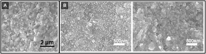
FIGURE 8. (A) SEM image of electrospray deposited Cs2TeI6 (scale 2 μm). Reprinted with permission. (Xu et al., 2018). Copyright 2019, ACS Photonics. (B) SEM images of electrospray deposited Cs2TeI6, without (left) and with (right) post deposition thermal treatment in a DMF atmosphere at 160°C for 5 h (scale 500 nm). Reprinted with permission (Guo et al., 2019). Copyright 2019, Journal of Materials Chemistry C.
The effects of spraying parameters on Cs2TeI6 film morphology was studied by Guo et al. (2019), who produced dense and compact thin films between 2 and 6 µm thick (Figure 8B). The authors varied the solvents, the jet electrical polarization and the substrate temperature. The films were deposited on mesoporous TiO2 and placed on aluminium foil under the syringe filled with the precursor solution and connected to a pump. The flow rate was set at 1 ml h−1. Solutions were prepared in DMF alone and in mixtures of DMF and n-butanol (1:1 v/v), DMF and IPA (1:1 v/v), DMF and ethanol (1:1 v/v), DMF and DMSO (1:1 v/v). The electrical polarizations applied were 6 kV, 8 kV, 10 kV and 12 kV. The substrate temperatures considered were: 145°C, 150°C, 155°C, 160°C and 165°C. After annealing, the samples were placed under a glass bell together with a 10 ml beaker filled with DMF and heated to 160°C for 5 h. The authors found that for a stable single conical jet, the electrical polarization to be applied is 10 kV. To find a suitable solvent, the authors evaluated the contact angle. A good surface wettability favours the growth of a smooth film. Furthermore, considering the boiling point of the solvent, they managed to obtain a dense film. DMF was found to be the most appropriate for wettability and evaporation rate. The nucleation rate influences the initial stage of film growth. To control it, the authors varied the substrate temperature. Evaluating the grains size, the film quality and crystallinity, the suggested temperature is equal to 160°C. DMF vapour treatment was implemented to improve the film quality. XRD analysis confirmed the formation of the pure phase with an indirect band gap of 1.88 eV (Guo et al., 2019).
Lead-based HPs have been brought to international prominence for their unique optoelectronic properties: high absorption coefficient, bright photoluminescence, balanced electron-hole mobility, tuneable exciton binding energy, and long exciton diffusion (Kang and Cho, 2020). Lead-based HPs, as stand-alone devices, are nowadays competing with established silicon photovoltaic (PV) technologies on efficiency. However, the presence of toxic metals and instability in air (Christians et al., 2018; Su P. et al., 2020), have pushed research towards replacing them with safer elements such as bismuth, which improves stability and reduces toxicity. So, the spotlight has turned to 0D HPds. Compared to 3D HPs, their 0D counterparts have optoelectronic properties that result from quantum confinement. For example, electron-hole pairs have higher binding energy than in 3D HPs, and therefore a higher photoluminescent efficiency, attractive for luminescence applications (Zhu and Zhu, 2020). Single-junction PV devices are limited in efficiency by the size of their band-gap relative to the solar spectrum. This is known as the Shockley-Queisser limit and it arises because photons with energy less than the band gap cannot be absorbed, and charge carriers excited by photons with energy exceeding the band gap lose a large portion of this energy through heat dissipation when charges relax thermally to the band edge before extraction. If photogenerated carriers could be extracted before they relax, the Shockley-Queisser could be exceeded. In nanostructures, this thermal relaxation is much slower due to phonon confinement, giving the possibility of hot carrier extraction (König et al., 2010). Therefore, developing such structures in bulk or thin-film self-assembled materials is highly desirable. Accordingly, it has shown that hot carriers last 10x longer in 2D HPs than in 3D HPs (Jia et al., 2018), inviting the possibility of hot carrier extraction from lower dimensional HPs. In this chapter, we start by analysing the results obtained in PVs, being the field that initially prompted the research on these compounds. After that, we address the promising results obtained using them in light-emitting diodes and laser. Finally, we describe their use as photodetectors. Applications are summarised in Figure 9.
FIGURE 9. (A) Cartoons of the main PV architectures: conventional (left) and inverted (right) (B) Schematic representation of a HP-LED. Reprinted with permission (Ji et al., 2021). Copyright 2021, Advanced Optical Materials. (C) Schematic representation of a HP-based laser diode. Reprinted with permission (Colella et al., 2016). Copyright 2016, The Journal of Physical Chemistry Letters. (D) HP photodetector architectures. Reprinted with permission (Gu et al., 2020). Copyright 2021, Advanced Optical Materials.
In 2009, the HP CH3NH3PbI3 was successfully employed as a sensitizer for electrochemical solar cells (Kojima et al., 2009). Only 3 years later, the efficiency of the PV devices was pushed up to 10%, using it as a light absorber layer in thin-film solar cells (Kim et al., 2012; Lee et al., 2012). Since that time, the race for high efficiencies has become feverish. In less than a decade, interdisciplinary collaboration and immense interest have pushed HPs to the current efficiency record of 25.6%, thus surpassing many other well-established technologies (such as CdTe and Cu(In,Ga)Se2) and flanking monocrystalline Si solar cells (Song et al., 2021).
The principal figure of merit of a solar cell is the PV efficiency, PCE, and this is defined as the efficiency with which the device converts solar irradiance into available electrical power. It is given by the ratio between the output and input power. The output power is obtained by multiplying the short-circuit current, Jsc, the open-circuit voltage, Voc, and the fill factor, FF. The FF is a measure of the deviation from the ideal case (FF = (Jmp Vmp)/(Jsc Voc), where Jmp and Vmp are respectively the current density and the voltage at the maximum power point) (Smets et al., 2016). Various device architectures were employed, but basically, they can be divided into two main categories related to the substrate conduction: n-type or p-type. The n-type configuration is commonly named the conventional architecture because it was the first employed. The electron transport material (ETM) is deposited onto a transparent conductive electrode (TCO) such as FTO. The ETM could be, for example, a single TiO2 compact layer or, alternatively, a bilayer in which a mesoporous TiO2 film covers the compact TiO2. The HP is grown on the ETM. The most common hole transport material (HTM) is spiro-MeOTAD, a small molecule primarily employed in solid-state dye-sensitised solar cells (DSCs) and organic light-emitting diodes (OLEDs). Nowadays, it is considered as the reference HTM for HP-based solar cells. In the p-type configuration, called inverted architecture, the TCO used is typically indium tin oxide (ITO), and the HTM (usually NiO or PEDOT:PSS) is deposited before the HP layer. Phenyl-C61-butyric acid methyl ester (PCBM) is commonly employed as ETM (Roy et al., 2020).
For a long time, however, the toxicity of lead-based HPs has worried researchers engaged in scaling up. Therefore, low-toxicity alternatives, such as Ge or Sn-based HPs, have been proposed. However, their easy oxidation in air limited their prospects. Bi seemed the ideal candidate to substitute Pb, in this scenario, due to its low toxicity and high chemical stability (Hu et al., 2017; Zhang L. et al., 2019). Park and collaborators tested bismuth-based hybrid HPs Cs3Bi2I9, (CH3NH3)3Bi2I9 and (CH3NH3)3Bi2I9-xClx in conventional solar cells, using spiro-MeOTAD as a hole HTM. The metal electrodes were made of silver. Cs3Bi2I9 provided the best performance with conversion efficiency higher than 1%, (FF = 0.60, Voc = 0.85 V, and Jsc = 2.15 mA cm−2); the authors attributed the low performance to the layer roughness and lack of compactness. Furthermore, they suggest that the charge transport materials employed are not the most suitable. However, stability tests revealed that Bi-based solar cells are stable for 1 month (Park et al., 2015b). Also, Singh and collaborators used (CH3NH3)3Bi2I9 as a light absorber in classical n-type architecture, reporting low but very stable performance (PCE = 0.2%, stable for 10 weeks under ambient conditions) (Singh et al., 2016). Devices prepared by Abulikemu and co-workers were also poorly efficient (PCE = 0.11%). According to the authors, the low efficiency was due to the film morphology and the inadequate alignment of the (CH3NH3)3Bi2I9 and HTM bands. Through the analysis of the surface photovoltage spectroscopy (SPS) data, the authors were able to calculate the mobility of the charge carriers (29.7 cm2 V−1 s−1) which is in the same order of magnitude as CH3NH3PbI3 (38 cm2 V−1 s−1). The trap density is also quite low, even lower than CH3NH3PbI3. Therefore, the authors attribute the low performance obtained to the high recombination of the photogenerated carriers, caused by the surface inhomogeneity and discontinuities (Abulikemu et al., 2016). Wang et collaborators tried to improve the surface morphology and thin film compactness using a two-step solution method, but the efficiencies produced did not go beyond 0.27%.
The authors once again stressed the critical importance of synthesising a stoichiometrically uniform, hole-free layer (Wang et al., 2017). On the other hand, Zhang and co-workers could make (CH3NH3)3Bi2I9 compact layers composed of large grains. They managed to achieve 1.64% conversion efficiency. The films seen in the cross-section appear compact, and the optimal thickness turned out to be 300 nm. The carrier lifetime was calculated from the transient PL decay measurements and ranged from 2.0 to 2.8 ns depending on the film thickness. The electron diffusion length was 189 nm, while that of the holes was 113 nm. Both are in the order of magnitude of those of the CH3NH3PbI3. Nevertheless, the charge mobility was found to be 7.91 × 10⁻⁴ cm2 V−1 s−1, which is four orders of magnitude less than CH3NH3PbI3. The authors attribute the low charge mobility to mixed conduction along with the crystallographic directions. In fact, along the c axis, there is a highly effective charge mass and relatively low dielectric constants (Zhang Z. et al., 2017). Also, Li and collaborators made a (CH3NH3)3Bi2I9 film with smooth, uniform, and compact surface morphology, but nevertheless they achieved the maximum conversion efficiency of just 0.33% (Li F. et al., 2019).
Exciting results came from solar cells in conventional architecture using the poly (3-hexylthiophene-2,5-diyl) (P3HT) as the HTM, even if the first attempt was not rousing (PCE = 0.19%) (Lyu et al., 2016). The authors attributed the poor efficiency to the large band gap and strong exciton binding energy. However, the device was stable for 40 days in air when exposed to humidity (50% RH) at room temperature (Lyu et al., 2016). But, later on, Jain and co-workers prepared the solar cells by depositing (CH3NH3)3Bi2I9 with a vapor-assisted technique on mesoporous TiO2 substrates, and P3HT as HTM. They managed to produce a record efficiency of 3.17%. The remarkable performance was attributed to the homogeneous surface coverage and improved stoichiometry. Solar cells only had a 0.1% drop in efficiencies in 60 days. The best devices provided a decent current density (4.02 mA cm−2), a good FF (0.78), and an impressive Voc of 1.01 V (Jain et al., 2018).
It should be noted that there have also been some attempts to replace TiO2 in bismuth-based HP devices, although not successful. When it was replaced with fluorinated perylene diimide, a maximum efficiency of just 0.06% was recorded (Huang et al., 2018). Chen and co-workers replaced the titania in anatase phase with a rutile TiO2 nanorod array. The best conversion efficiency (0.14%) was obtained with a titania thickness of 564 nm. The authors attribute the poor PV performance to the surface roughness and the high exciton binding energy (Chen M. et al., 2018).
Even when 0D HPds were used in inverted architecture, performances that could be competitive with 3D HPs was not obtained. Öz used the p-type architecture: ITO/PEDOT:PSS/HP/PC60BM/Ca/Al. The conversion efficiency obtained was 0.1%. The authors stated that the low conversion efficiency was due to the large band gap (2.9 eV) and the inadequate alignment of the energy levels of the charge transport materials. Furthermore, they pointed out that the low short circuit current was caused by the configuration used, failing to split the exciton with a binding energy of 400 meV (Öz et al., 2016). Baranwal and co-workers compared different HP compositions based on bismuth and antimony in conventional and inverted architectures (Baranwal et al., 2017). Since the substrate impacts the growth of the layer itself (Trifiletti et al., 2018), the performance in the final device is also different. The best performance for the hybrid compositions was obtained with (CH3NH3)3Bi2I9 in the conventional configuration, thanks to better substrate coverage (Baranwal et al., 2017). In inverted architecture, a performance of 0.39% has been achieved. Again, the low performance was attributed to the strong exciton binding energy. However, the authors added that other detrimental effects are the short carrier diffusion length, their low mobility, and the high density of the trap states (Ran et al., 2017). Even the deviation from the pristine Bi-based compound could not increase the PV performances: (CH3NH3)6BiI5.22Cl3.78 reached a maximum conversion efficiency of 0.18% (Hoefler et al., 2018), and (CH3NH3)3Bi2I9-2xSx achieved an efficiency of 0.15% (Li et al., 2019c).
Unfortunately, also, the HP based on Sb could not provide performances comparable with their lead-based counterparts. Solar cells in a p-type configuration, have been manufactured using (CH3NH3)3Sb2I9, obtaining a maximum power conversion efficiency of 0.5%. The low maximum EQE value, 12%, indicates that charge carrier collection in this architecture is inefficient (Hebig et al., 2016). An important result, which could open up new study paths, was reported by Chatterjee and Pal (2018). They completely revolutionized the components of the device, adapting them to the light absorbing layer. Thus, they obtained a PCE of 2.69% with a (CH3NH3)3(Sb0.6Sn0.4)2I9-based solar cell, in the configuration: ITO/Cu:NiO/HP/ZnO/Al. The optimum Sb:Sn ratio in terms of band gap and surface roughness was found to be 6:4. STS studies established good band alignment with both Cu:NiO and ZnO. Pristine Sb-based HP provided a maximum conversion efficiency of 0.57%. In devices employing HP substituted with Sn, the current increases as the tin content increases, thanks to the band gap narrowing, which increases the photogenerated charge. In addition, band tuning can promote the alignment with the charge transport materials’ bands, improving charge extraction and, therefore, the FF. Also, the decrease in Voc is a consequence of the band gap narrowing. Increasing the Sn amount over 40%, the PV parameters were lowered due to an increase in the charge carriers’ recombination. Moreover, a notable increase in roughness and impurities occurs, acting as recombination centres for the charge carriers. The devices were left in air for 15 days, at an average temperature of 24°C and average relative humidity of 60%. Samples with Sn-doped 0D HPd saw performance drop by 80%, while those with pristine Sb remained stable. Since the XRD spectra did not show HP degradation processes, the authors attribute the loss to the Al contact degradation. The devices stored in glove boxes, on the other hand, maintained their initial performance (Chatterjee and Pal, 2018). Some of the same authors studied the effect of bandgap variation with composition modulation in (CH3NH3)3(Sb1-xBix)2I9. The best conversion efficiency, 1%, was obtained for (CH3NH3)3(Sb0.4Bi0.6)2I9, which generates the best balance between surface roughness, bandgap, and excitons binding energy (Chatterjee et al., 2020).
The few reports on Cs3Sb2I9 faced the same limits of the hybrid compounds. Correa-Baena and co-workers tested it in conventional architecture solar cells. Despite the excellent surface roughness, the devices showed low photocurrents (0.1 mA cm−2) and PCE (0.03%). The authors blame the large exciton binding energy, therefore the high degree of charge confinement in the low dimensional structures, and the large carrier effective masses (m*h = 1.55 and m*e = 1.40; calculated from DFT) (Correa-Baena et al., 2018). Singh and collaborators compared the Cs3Sb2I9 0D and 2D form and employed them in reverse architecture solar cells. Notably, the best result (0.89%) for the 0D structure was obtained by removing the HTM, with the aluminium contact directly deposited on the HP film, to raise the short circuit current. The authors explain this with a mirror effect from the back contact, which enhances the light collected (Singh et al., 2018).
Later on, also Peng et al. compared the two phases in the conventional architecture: spiro-MeOTAD was substituted by poly (N,N′-bis-4-butylphenyl-N,N′-bisphenyl)benzidine (poly-TPD). The 0D Cs3Sb2I9 absorber gave an efficiency of 0.24%, meanwhile the 2D Cl-substituted Cs3Sb2Cl3I6 reached a PCE value of about 1.56% (Peng et al., 2020).
In Table 4, the PV parameters of the reviewed devices are listed. Even in the best performing device (Jain et al., 2018), where the Voc and FF are comparable with the lead-based HPs devices, the current density is relatively low. As highlighted in this section, even when a pin-hole free layer is deposited, the large optical band gap and the high exciton binding energy dramatically limit the application of the 0D HPds in PV, although the motivation to replace lead ensures that work in this area is ongoing. Recently (Peng et al., 2021), their low toxicity and large band gap have been motivating the investigation of these compounds as indoor light harvesters. The bandgap values around 2 eV are, indeed, optimal for indoor PV, because the spectra of indoor light sources are blue-shifted compared to the reference spectrum used for outdoor PV (Peng et al., 2021).
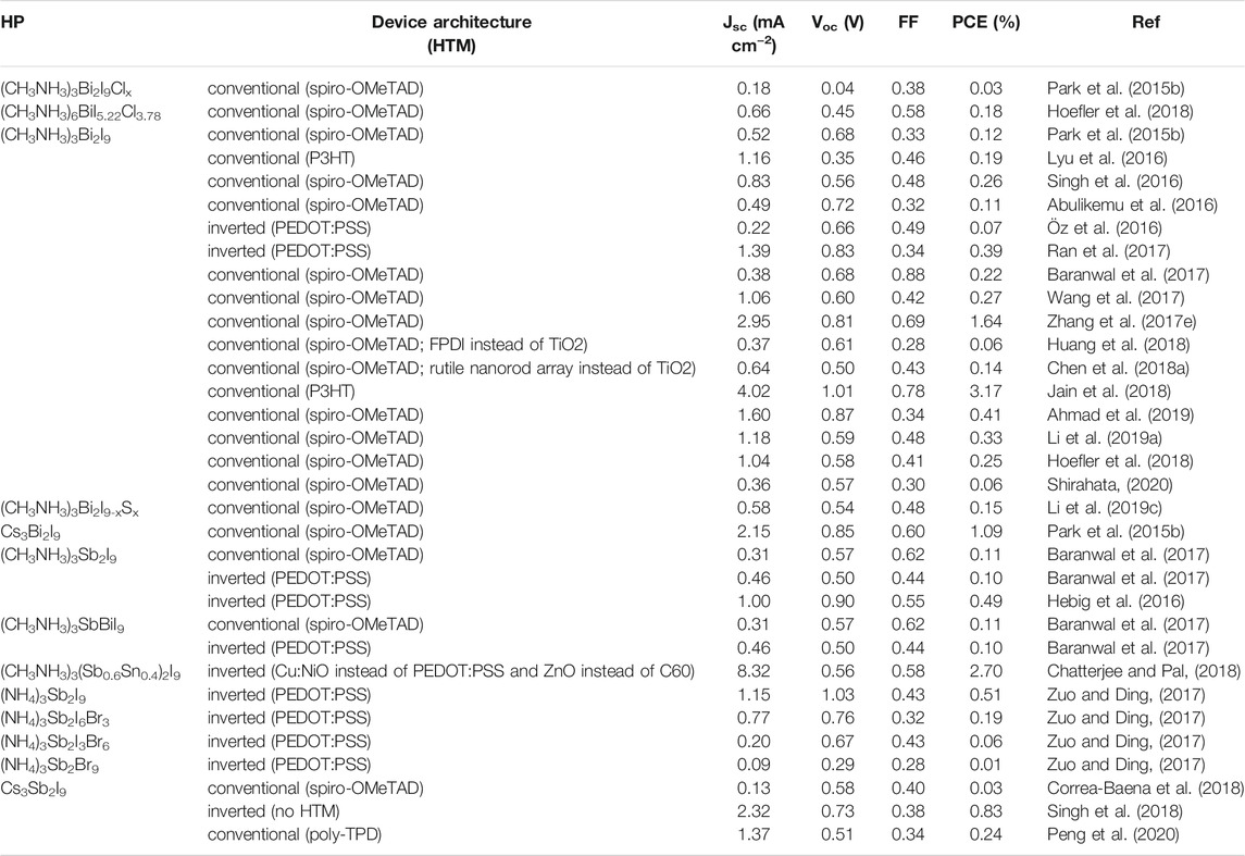
TABLE 4. Summary of PV parameters, in the reverse scan direction, of the champion devices published employing 0D HPds.
Light-emitting diodes (LEDs) are used in solid-state lighting (SSL) applications to convert electricity into light (Tsao and Coltrin, 2006). Today, SSL is used in our homes, streets, and many technological devices due to its high energy efficiency, low cost, low energy consumption, and long lifetime compared to conventional lighting sources such as fluorescent, high-intensity discharge lamps or incandescent (De Almeida et al., 2014). The performance of LEDs and thus the efficiency of SSL strongly depends on the material used in the active region (or light-emitting layer). The active region should exhibit high internal quantum efficiency (or quantum yield) (IQE) and the device as a whole should achieve a high external quantum efficiency (EQE). These two quantities are proportional to each other, modulated by the probability of injected charges combining in the active region and the probability of a generated photon from the active region exiting the device. The other important parameters for the determination of LED performance are stability, maximum luminance, power efficiency (PE), current efficiency (CE) and turn-on voltage (Van Le et al., 2018). Work on HP-based LEDs began with the mixed halide 3D HP, CH3NH3PbI3–xClx, in 2014 (Tan et al., 2014), and HPs are now considered as promising candidates for LEDs due to their widely tuneable bandgaps, high photoluminescence quantum yield (PLQY) and high charge carrier mobilities (Colella et al., 2016; Liu et al., 2021). 3D HP-based LEDs with high EQE of 10.43% and brightness of 91,000 cd m−2 were prepared by using green-emitting inorganic CsPbBr3, mixed with a small amount of organic methylammonium cation (Zhang L. et al., 2017). Nevertheless, the device’s instability caused significant decay of efficiency and brightness within a few hours. 3D HPs suffer from instabilities, either inherent or triggered during device operation (Almutlaq et al., 2018b). On the other hand, low dimensional HPds (corrugated-2D, 1D and 0D) provide higher stability as well as broadband emission due to efficient exciton self-trapping in quantum-confined structures (Zhou et al., 2017; Zhang F. et al., 2020; Liu et al., 2020b). Though HP nanocrystal-based LED devices achieved great successes, their fragility and difficult fabrication process limit their usability (Chen X. et al., 2018). Large-size crystals offer higher stability and ease the fabrication process. However, their high density of traps and defects and long exciton diffusion lengths result in weak PLQE (Stranks et al., 2014). Saidaminov et al. synthesized pure Cs4PbBr6 microcrystals which exhibited PLQY (45%) of two orders of magnitude higher than 3D CsPbBr3 (Saidaminov et al., 2016). Later on, Chen et al. reported centimetre sized Cs4PbBr6 crystals with embedded CsPbBr3 nanocrystals as green emitters with extremely high PLQY (97%) and good thermal stability. They explored the use of Cs4PbBr6 crystals with embedded CsPbBr3 nanocrystals for wide colour gamut WLEDs (white light-emitting diodes) (Chen X. et al., 2018). Chiara et al. presented Cs4SnBr6 NCs that emission in the green region of the visible spectrum with a PLQY (∼65%) higher than those of the corresponding tin-based 3D HPs (Jellicoe et al., 2016; Chiara et al., 2020). Cs3Cu2I5 HP materials are considered good candidates in light-emitting applications as they are lead-free, air-stable and non-toxic (Jun et al., 2018). Single crystals of Cs3Cu2I5 with high PLQY (89% for crystals and 60% for powder) were prepared by Zhang et al. Cs3Cu2I5 powder served as a blue-emitting phosphor in UV pumped down conversion LEDs, while the precursor solution of these Cs3Cu2I5 crystals was used as a fluorescent ink. In addition to that, they used direct laser writing technology to demonstrate the ability to produce patterned composite Cs3Cu2I5/PVDF (polyvinylidenefluoride) films for displays applications (Zhang F. et al., 2020). In another study reported by Jun et al. Cs3Cu2I5 blue emitting materials exhibited similar PLQYs (91% for single crystal and 62% for thin film) and were incorporated into blue LEDs (Jun et al., 2018). Roccanova et al. reported Cs3Cu2Br5−xIx (0 ≤ x ≤ 5) polycrystalline powders, which showed bright blue emission. Cs3Cu2Br5−xIx (0 ≤ x ≤ 5) single crystals showed high PLQY ranging from ∼99 to 50% with descending values of x. They also noted that the small variation between all reported PLQY values of Cs3Cu2I5 might be due to the different synthesis method and the purity of the compounds (Roccanova et al., 2019). Cs3Cu2Br5 and Cs3Cu2I5 showed ambient stability over 1 month. Recently, 0D HPds are also considered efficient light-emitting materials due to their host-guest systems where light-emitting species are localized in an inert host matrix (Zhou et al., 2018c). Zhou et al. synthesized (C9NH20)2SnBr4 light-emitting bulk crystals as efficient broadband deep-red emission and with a quantum efficiency of around 46% (Zhou et al., 2018b). Subsequently, they reported perfect host-guest concepts with single crystalline materials (C4N2H14X)4SnX6 (X = Br or I) and (C9NH20)2SbX5 (X = Cl). Gaussian-shaped and strongly Stokes shifted broadband emissions with extremely high photoluminescence quantum efficiencies (PLQEs) of 95 ± 5% for (C4N2H14Br)4SnBr6, 75 ± 4% for (C4N2H14I)4SnI6 and 98 ± 2% for (C9NH20)2SbCl5) were obtained. The WLED consisted of yellow emitting (C4N2H14Br)4SnBr6 blended with commercial blue emitting europium-doped phosphor (weight ratio of 1:1). It showed decent white emission with colour rendering index (CRI) of 70 and great stability in air, without any change of light brightness and colour for more than 6 hours (Zhou et al., 2018a; Zhou et al., 2018c). Later on, the same group reported the 0D tin-based mixed-halide HP (C4N2H14Br)4SnBrxI6–x (x = 3) with much broader yellow emission but lower PLQE of ∼85% than that of (C4N2H14Br)4SnBr6. WLEDs, made of the yellow phosphor (C4N2H14Br)4SnBrxI6–x blended with a europium-doped blue phosphor, showed a higher CRI of 85 due to the extended emission of this yellow phosphor into the visible red region. They also showed good stability in air with minimal change in the emission colour for more than 12 h (Zhou et al., 2017). Another efficient light-emitting 0D material, (Ph4P)2SbCl5 with high thermostability, was reported by Zhou et al.: single crystals exhibited yellow emission with close to the unity PLQE of 99 ± 1% (Zhou et al., 2018d). Wang et al. prepared [Bmim]2SbCl5 (where Bmim is 1-butyl-3-methylimidazolium) polycrystals and thin films which exhibited tuneable yellow/white emission with quantum efficiencies of 86.3 and 82.6% for polycrystals and thin film, respectively. When the excitation wavelength is about 250 and 450 nm, the compound emits in the yellow range, meanwhile with an excitation wavelength of 350 nm the emission is white [Bmim]2SbCl5 containing LEDs were demonstrated as a temperature sensing colour changing LED that may be used as a high-temperature warning device (Wang Z.-P. et al., 2015). Green light-emitting diodes containing 0D (Ph4P)2(MnBr4), was prepared by Xu et al. for OLED applications (Xu et al., 2017). The compound displayed high thermal stability without degradation (higher than 400°C) with an EQE of 7.2 and 9.6% (for non-doped four-layer OLEDs and doped three-layer OLEDs, respectively) that are higher than usual external efficiency (less than 5%) (Hui, 2020). (1-C5H14N2Br)2MnBr4 single crystals were synthesized as potential materials for light emitting applications. These green phosphors exhibited PLQY of 60.70% and thermal stability up to 300°C (Jiang et al., 2020).
In summary, the outstanding optical and charge transport properties of 0D HPds have enabled their use as the active layer in rather efficient LEDs. This field is relatively young compared to HP PVs, and it is expected that, with further investigations and experimental effort, these materials could be widely used in future light emitting applications such as lighting, phototherapy, and indoor farming (Bispo-Jr et al., 2021; Li et al., 2021b).
In materials capable of laser emission, the generated radiation, coherent and nearly monochromatic, comes from the amplification of a stimulated emission using confinement of the active material in a cavity or a periodic structure. The laser beams are closely collimated and can have high power; therefore, they are widely used in scientific research and various technological fields, such as health care and telecommunications. Research on semiconductor lasers has led to the development of micro- and nano-lasers for high-speed communication and display devices. However, industrially applicable semiconductor lasers (InP, GaN and GaAs) involve rare elements and are produced by expensive methods (CVD and molecular beam epitaxy) (Zhang Q. et al., 2021). In the last twenty years, research on organic semiconductors has opened the study of an alternative and low-cost production way, although the poor electrical properties hinder their industrial development. In this context, research on the lasing properties of HPs was born, with both green and red lasing having been observed at room temperature (Zhang Q. et al., 2021). However, 3D HPs usually have weakly bonded excitons, which is advantageous for PV applications, but it is a limitation for achieving high electroluminescence efficiencies. On the other hand, a not too high binding energy favours good charge transport. So, to have an efficient emission, the excitons should be confined, and recombination should occur within short time regimes (Colella et al., 2016). To do this, the most followed approach is to try to reduce the system dimensionality by engineering the chemical composition, the particle size or employing nanocrystals acting as quantum dots (Colella et al., 2016; Stylianakis et al., 2019). Lately, Sun and co-workers studied the 0D HPds Cs4PbBr6, and they pointed out that the compound has the advantage of suppressing the photoluminescence, which reduces the emission in the 3D HPs. The sharing of octahedra in three-dimensional structures limits the confinement of the charge. In the 0D HPds, the partial isolation of the octahedra of [PbBr6]4− leads to the higher binding energy of the excitons (Sun et al., 2019). The authors state that green emission is intrinsic to the material because it is correlated to the localized optical absorption of Pb2+ in the isolated octahedra. Upon optical pumping, they demonstrated the presence of single and multimode laser resonances and used the emission to obtain good images of micrometric objects (Sun et al., 2019).
The 0D HPds application in lasers is in infancy, but the first results are promising. They can self-assemble into materials with quantum confinement characteristics, and the exciton binding energy in 0D compounds can be modulated by varying the chemical composition. For electrically-pumped lasing, the charge mobility can be tuned by engineering the synthesis method as described in earlier chapters of this review.
Photodetectors (PDs) are sensors that transform optical into electrical signals and are widely used in imaging, optical communications, and motion detection (Nasiri and Tricoli, 2019). Compared to conventional PD materials, such as Si and groups III-V compounds, solution-processed HPs are more easily produced and the lead-free versions can be considered more environmentally friendly (García de Arquer et al., 2017). Previous reports have shown many attractive properties of 3D HPs, which justify their potential for photodetection use (Fang and Huang, 2015; Bao et al., 2018; Wu et al., 2019). However, the photocurrent hysteresis, caused by the ion migration assisted by grain boundaries (Seol et al., 2017), reduced the reliability and moisture stability of 3D HPs, limiting their practical applications. 0D HPds, including QDs, NCs, and nanoparticles (NPs), have tenable sizes, significant extinction coefficients, high PLQYs with narrow emission bandwidth and better stability than their 3D counterparts. All these properties make them potential candidates for photodetector applications (Shang et al., 2019; Wang H. P. et al., 2021). Generally, HP-based photodetectors can be divided into two-terminal (photodiodes and photoconductors) and three-terminal devices (phototransistors) (Gu et al., 2020). Many parameters define the characteristics of photodetectors such as responsivity (R), detectivity (D*), noise equivalent power (NEP), linear dynamic range (LDR) and response speed (Dou et al., 2014). The desired performances can be different according to the application. Generally, photodiodes should have a low driving voltage and a fast temporal response due to an engineered p-n or p-i-n junction and a narrow electrode spacing (Shang et al., 2019). They should also have low dark current due to the junction barrier. However, they usually show low EQE and low responsivity since photodiodes with blocking/rectifying contacts do not undergo additional charge injection under reverse bias. Contrarily, photoconductors and phototransistors usually have high EQE and responsivity with high driving voltage and slow temporal response due to the large electrode spacing.
Low dimensional HPs have been extensively tested for photodetection (Wang Y. et al., 2015; Saidaminov et al., 2016; Bessonov et al., 2017; Li et al., 2017; Gui et al., 2019; Liu T. et al., 2020; Chen J. et al., 2020; Wang H. P. et al., 2021). Those based on iodine or bromine have response located in the visible region due to the bandgap which is typically less than 2.5 eV. Those based on chlorine have a wider bandgap, so they can be used in UV or near-ultraviolet (NUV) detection. Unfortunately, the poor quality of the films hindered the charge transport (Gui et al., 2019). Gui et al. synthesized single crystals of CsPbCl3, which demonstrated an R of 0.45 AW-1 at 5 V for NUV, with an on/off ratio of 5.6 × 10³ (Gui et al., 2019). Thanks to the high crystallinity, both the noise and the dark current are low, while D* is of the order of 1,011 Jones. However, the performance of photodetectors based on 0D HPds is limited by the strong excitonic bond, which makes it challenging to extract the charge. It is possible to modify the surfaces and control the structure to overcome these limitations. Some authors have, for example, passivated the surface to reduce interface defects (Pan et al., 2016; Koscher et al., 2017; Pan et al., 2018; Gong et al., 2019). Furthermore, manipulation of the morphology or size of the synthesized compounds can increase the lifetime of the charge carriers and the diffusion coefficient (Saidaminov et al., 2016; Liu X. et al., 2017; Yang et al., 2017; Li et al., 2018; Zhang et al., 2018). The micrometric HC(NH2)2PbBr3 crystals synthesized by Zhang et al. (2018) have a low trap density (6.98 × 1011 cm−3). The CsPbBr3 microcrystals synthesized by Yang et al. (2017) have a good trap density (1012 cm−3) and remarkable charge mobility (100 cm2 V−1 s−1). Thanks to efficient charge transfer, CsPbBr3 has an R of 6 × 10⁴ AW−1, a fast response time of about 1 ms, a D* value of 1013 and a gain of 105 (Yang et al., 2017).
Therefore, photodetectors based on 0D HPds have the advantage of having a light collection comparable with 3D HPs, but the most important challenge is improving the charge extraction to make them competitive with conventional materials. In addition, unique features might be possible to implement, such as direct linearly or circularly-polarised light detection that can be induced by nano-structuring (Gao et al., 2016) or by incorporation of chiral organic cations (Chen C. et al., 2019; Wang L. et al., 2020; Ishii and Miyasaka, 2020).
In the mid-20th century, the shift to an information driven economy pushed society into the so-called information age. Common and industrial electronic devices have had to adapt to meet the demands of faster data processing, higher density storage, lower energy consumption, multifunctionality, flexibility, scalability and simple, economical and eco-friendly production (Choi et al., 2018). Since silicon, unfortunately, cannot meet all these demands, research on materials science and engineering has explored various paths, such as the use of organic semiconductors, metal oxides and low-dimensional materials (Orton, 2009). HPs have been shown to have electronic properties that can be easily controlled with the composition or deposition method, which in general guarantees simple and compatible fabrication with flexible electronics (Lee et al., 2021). In particular, 0D HPds have certain properties that make them interesting to investigate in devices beyond optoelectronics, for reasons that will be outlined below. This section focuses on recent advances in radiation detectors, memristors, capacitors, and thermal energy harvesters and thermal sensors, Figure 10).
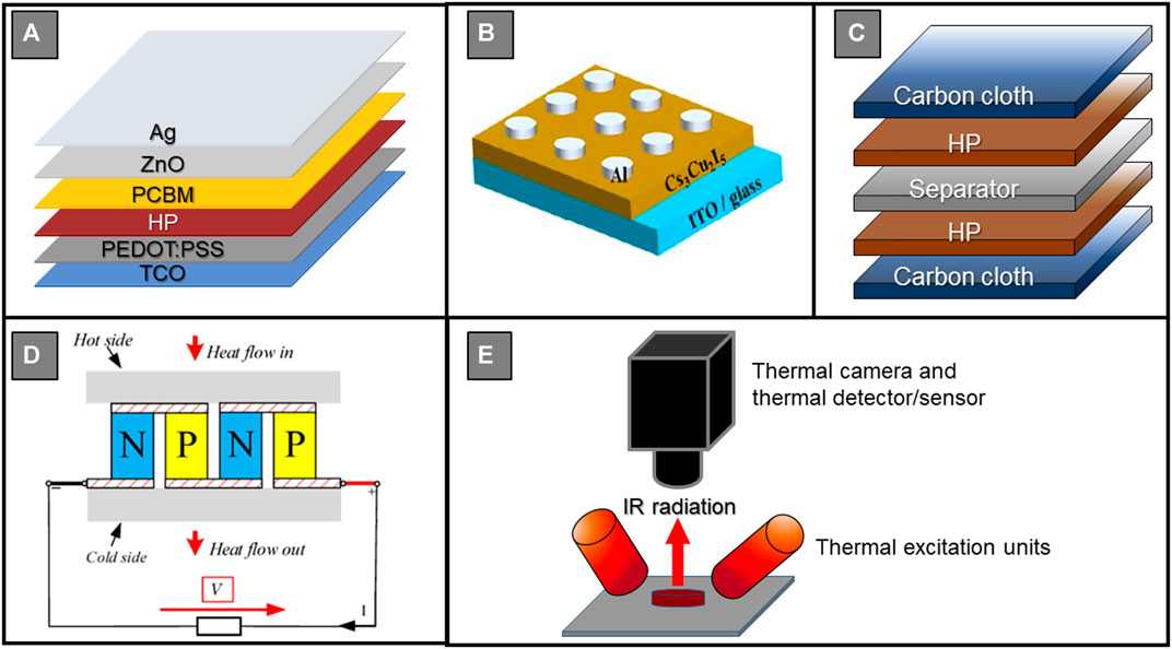
FIGURE 10. (A) Device stack of a HPs-based X-ray detector. (B) HP-based resistive switching random access memory (ReRAM) device. Reprinted with permission (Zeng et al., 2021). Copyright 2021, The Journal of Physical Chemistry Letters. (C) Cartoon of a HP-based symmetrical capacitor. (D) General structure of a thermoelectric generator (TEG). Reprinted with permission (Siouane et al., 2017). Copyright 2017, Energies. (E) Scheme of a thermal imaging system.
X-ray detectors are essential for various applications such as medical radiography, industrial inspection, and security screening (Zheng et al., 2020). X-ray detection is provided either by directly converting X-ray photons into electronic signals (Zhang et al., 2020c), or by indirect conversion using scintillators that convert X-ray photons into UV-visible photons (Li Y. et al., 2019). The broad range usability of X-ray detectors, especially in therapeutic radiation, has motivated researchers to minimize X-ray dose rate (or limit of detection, LoD) by developing high-sensitive X-ray detectors. A high signal-to-noise ratio is needed, which is related to low dark current (high resistivity). 3D HPs have shown improved sensitivity compared to conventional X-ray detectors, but they are limited by long-term operational stability due to their high dark carrier concentration and ion migration (Zheng et al., 2020). On the other hand, 0D HPds may remove this limitation as isolated metal-halide units prevent ion migration and provide more localized electronic structures resulting in low dark current. HP single crystals offer a platform to study intrinsic optoelectronic properties for X-ray detection due to their low defect density and grain boundary-free properties (Xu X. et al., 2020). Recently, Zhang et al. (Zhang et al., 2020c) synthesized all-inorganic HP Cs3Bi2I9 single crystals (12 mm × 12 mm x 3 mm) by nucleation control growth method. The single crystal exhibited large resistivity of 2.8 × 10¹⁰ Ω cm, and a high μτ product of 7.97 × 10⁻⁴ cm2 V−1 leading to a sensitivity of 1,652.3 μC Gyair−1 cm−2, which is about 4 times higher than conventional α-Se detectors (440 µC Gyair−1 cm−2), with LoD of 130 nGyair−1 s−1, that is two orders of magnitude lower than state-of-the-art 3D CH3NH3PbI3 single crystals (19.1 µGyair s−1) (Zhang et al., 2020c). Very recently, Xu et al. synthesized a very sensitive and stable 0D Cs4PbI6 single crystal with a μτ product of 9.7 × 10⁻⁴ cm2 V−1 and 451.49 μC Gy−1 cm−2 (Xu et al., 2021). Moreover, having all-inorganic components instead of volatile organic cations gave rise to high operational and thermal stability. Liu et al. (2020c) reported higher carrier mobility-lifetime (μτ) (2.87 × 10⁻³ cm2 V−1) with 0D (CH3NH3)3Bi2I9 single crystals (26 mm × 26 mm × 8 mm) grown by the same strategy. The single crystals with excellent operational stability had a similar resistivity of 3.74 × 10¹⁰ Ω cm, and the detector generated higher sensitivity of 1947 μC Gyair−1 cm−2 but a lower LoD of 83 nGyair s−1. They also revealed that 0D (CH3NH3)3Bi2I9 showed the lowest dark current (∼8 pA), compared with the 2D (PEA)2PbI4 (∼41 pA) and 3D CH3NH3PbI3 (0.5 μA). Similarly, Zheng et al. (2020) performed measurements on 0D (CH3NH3)3Bi2I9 single crystals (27 mm × 23 mm × 13 mm), which exhibited extremely large resistivities of 5.27 × 10¹¹ Ω cm (out of plane) and 5.52 × 10¹⁰ Ω cm (in-plane) with suppressed ion migration. The carrier mobility lifetimes (μτ) for out-of-plane and in-plane directions were obtained as 2.8 × 10⁻³ and 1.2 × 10⁻³ cm2 V−1, respectively. The detector generated a high sensitivity of 10,620 μC Gyair−1 cm−2 (out-of-plane), which is in the same range as state-of-the-art 3D CH3NH3PbI3 (1.1 × 10⁴ μC Gyair−1 cm−2), with LoD of 0.62 nGyair s−1. Low dark current resulted in LoD of 0.62 nGyair s−1, which is 8,800 times lower than the dose rate required for X-ray diagnostics used currently and is the lowest value among all reported HP-based X-ray detectors. It also showed outstanding operational stability under high bias and high X-ray dose (∼24 mGyair).
On the other hand, polycrystalline HPs are favourable from a processing perspective since they can be readily deposited over a large area. A high electric field can be applied to the detector, eliminating the signal cross-talk between neighbouring pixels as charge transport materials can be assembled at both sides of polycrystalline HPs (Xu X. et al., 2020). Recently, a 0D Cs2TeI6 all-inorganic HP film was grown by the electrospray method for X-ray detection with high stability (Xu et al., 2018; Guo et al., 2019). The resistivity of well-defined, thick films was increased from 4.2 × 10¹⁰ Ω cm to 5.06 × 10¹⁰ Ω cm by tailoring the electrospray parameters such as electric field, solvent, temperature. The resistivities were lower than in its single crystal form that was 9.92 × 10¹¹ Ω cm. The higher resistivity of single crystals was attributed to the low defect density compared to polycrystal thick films. The formation energy of defects such as iodine vacancies, linked to the shallow-level defects (source of free charge carriers), is higher in single crystals, so their formation is hindered (Xiao B. et al., 2020). The Cs2TeI6 single crystal-based device shows an X-ray sensitivity of 27.8 μC Gy−1 cm−2 and a LoD of 72.5 nGy s−1. However, they showed lower sensitivity than Cs2TeI6 single crystals (27.8 μC Gyair−1 cm−2 at 2.76 V mm−1) with values of 192 nC R−1cm−2 under 40 kVp X-rays (19.2 μC Gyair−1 cm−2 at 40 V mm−1) and the charge mobility-lifetime (μτ) was measured as 5.2 × 10⁻⁵ cm2 V−1 that is relatively lower than aforementioned 0D HPd single crystals. Table 5 summarizes all 0D X-ray detector’s key parameters made of single crystals and polycrystalline HPds.
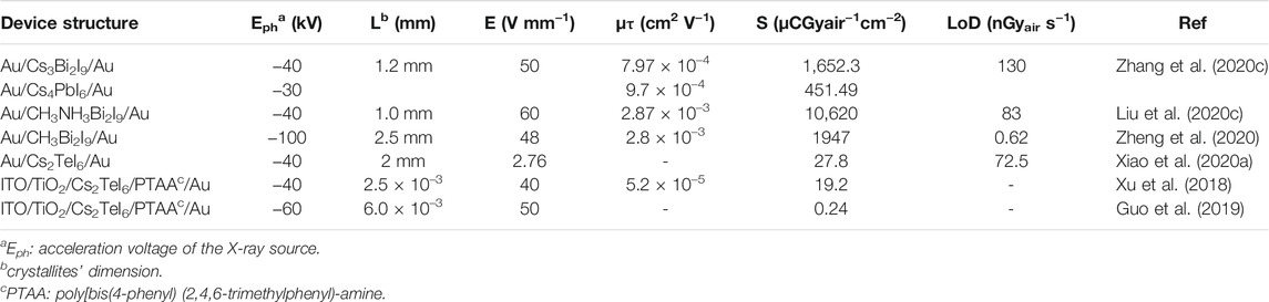
TABLE 5. 0D HPd X-ray detectors’ key parameters made of single crystals and polycrystalline 0D HPds.
In conclusion, recent studies showed that 0D HPds might be the right candidate for X-ray detection applications. However, there are relatively few reported studies on 0D HPd-based X-ray detectors to date. To better understand the efficacy of these HPs in X-ray detection, novel compounds are needed to be developed. Besides that, the application of single crystals is limited to the small active area due to their sizes, and other technologies should be developed to use single crystals in commercial devices. On the one hand, it is challenging to fabricate polycrystalline materials with high uniformity and adequate thicknesses, which affect the sensitivity and X-ray attenuation, respectively (Xu X. et al., 2020). Additionally, the defect effects of polycrystalline films have not been well-understood. Thus, many scientific efforts are needed for the fabrication of commercial 0D HPd-based X-ray detectors.
Besides X-ray detectors, HPds are used as scintillators due to their favourable detection efficiency, high energy response, and large absorption cross-section (Zhou F. et al., 2020). More specifically, this is due to their efficient luminescence, high stability, and considerable X-ray stopping power enabled by little to no self-absorption (Zhou C. et al., 2020; Zhou et al., 2021). Recently, studies focused on developing new HPd scintillators with high irradiation yield and sensitivity (He et al., 2020). For example, Cao et al. (2020) increased the sensitivity and stability of CsPbBr3 scintillators by employing emissive NCs embedded in a Cs4PbBr6 thin film (CsPbBr3@Cs4PbBr6), fabricated by a blade-coating technique. Similarly, Xu Q. et al. (2020) reported the same composition, which exhibited high light yield and long term stability in air. Cs3Cu2I5 single crystals synthesized by Cheng S. et al. (2020) demonstrated high light yield, 32,000 photons MeV−1 and a low afterglow of 0.03% at 10 ms under X-ray radiation, something that is required for high-quality images. Moreover, they exhibited a light yield of 29,000 photons MeV−1 under gamma-ray radiation. Furthermore, Yuan et al. discovered that doping of Cs3Cu2I5 with 1% Tl resulted in a higher light yield of ∼51,000 MeV−1 due to the self-trapped excitons and Tl centres. Tl is already widely used as doping in commercial halide single-crystal scintillators (e.g. NaI:Tl, CsI:Tl), to widen the broadband emission: the pristine compound showed a single blue emission, correlated to the STEs, meanwhile the Tl-doped crystal had an emission covering the visible range, with stronger luminescence intensity (Yuan, 2020). Cs3Cu2I5 nanocrystals prepared by Lian et al. with the drop-casting method resulted in large-area, self-absorption free with an extremely high light yield of 79,279 photons MeV−1 scintillators (Lian et al., 2020). Cs4EuBr6 and Cs4EuI6 single crystals prepared by Wu et al. also demonstrated high light yields; 78,000 ± 4,000 photons MeV−1 and 53,000 ± 3,000 photons MeV−1 under gamma-ray irradiation, respectively (Wu et al., 2018). Rustrom et al. reported Eu2+ doped (7%) Cs4SrI6: Eu and Cs4CaI6: Eu single crystal scintillators, which exhibited similar results as scintillators as mentioned above; the light yields of Cs4SrI6:Eu and Cs4CaI6:Eu were 71,000 photons MeV−1 and 69,000 photons MeV−1, respectively (Rutstrom et al., 2019). Recently, He and co-workers reported (PPN)2SbCl5 (PPN = bis(triphenylphosphoranylidene)ammonium cation) single crystals with relatively lower light yield of 49,000 MeV−1, however remarkable stability under ambient conditions even after 2 years. They also displayed a much lower detection limit (191.4 nGyair s−1) than required for medical diagnostics (5.5 μGyair s−1) (He et al., 2020). Lastly, the same group developed a (C38H34P2)MnBr4 single crystal scintillator, which exhibited a superior light yield of about 80,000 photons MeV−1 with a much lower detection limit 72.8 nGyair s−1. (C38H34P2)MnBr4 based flexible scintillators with a high spatial resolution (0.322 mm) could be prepared by blending (C38H34P2)MnBr4 powder and polydimethylsiloxane (Xu L. J. et al., 2020). All reported studies showed that 0D HPd materials are excellent candidates for irradiation detection applications. However, further investigations need to be conducted to optimise them for future applications, such as in the field of medical imaging. In this sector, the use of inaccurate detectors requires to increase radiation dose and exposure times in order to have an accurate diagnosis, thus increasing the risk for the patient. 0D HPds could make a difference in developing the new X-ray detection devices, cheaper and with improved performance, that are demanded by the market and society.
Memristors (i.e., memories plus resistors) have the potential to be the basis for data-centric computing technology, substituting the transistor and capacitor based systems currently in place. A memristor is a passive two-terminal device formed of an insulating or semiconducting material sandwiched between two electrodes. It has resistance states that application of an electric field can tune. Two principal memristor mechanisms have been identified: conductive filament (CF) and the memristive interface mechanisms. The CF mechanism occurs when conduction pathways form or annihilate in the insulating layer, under an applied field. If a CF bridges the electrodes, a low resistance state (LRS) is formed, and if the CF recedes, a high resistance state (HRS) is formed. The memristive interface mechanism occurs when the Schottky contact between the semiconductor and the electrode is modulated. In this case, the LRS is reached when ion migration (or charge trapping/de-trapping) reduces the build-in potential. Conversely, the HRS is achieved when a reverse bias is applied to inject charges and recover the Schottky barrier. The two primary memristor operations depend on the resistance switching type. Discrete switching between HRS and LRS allows digital operation, with applications in non-volatile memory for information storage and logic operations, requiring highly stable resistive switching. Continuous switching delivers continuously tuneable resistance states and analogue operation; devices resemble biological synapses and have application in novel neuromorphic computing systems. The repeated annihilation and formation of filaments affects the cycle-to-cycle variability and cycling endurance. These deviations from ideal behaviour prevent achievement of high accuracy and need to be addressed to push memristor technology to maturity. (Joksas et al., 2020).
HPs have been regarded as promising materials for memristors, thanks to their mixed ionic-electronic conduction (Xiao et al., 2015). Whilst ion migration in HPs solar cells has been a significant issue (Snaith et al., 2014; Trifiletti et al., 2016), the phenomenon can be exploited to generate the memristive behaviour. Moreover, HP-based memristors can pave the way to investigate novel functions such as light accelerated learning capacity, thanks to efficiently light harvesting. Light illumination was found to produce a tuneable memristive behaviour, enabling multilevel logic applications well suited for sensor networks (Zhao et al., 2019). The most studied 3D HP is CH3NH3PbI3, but it shows poor air stability and high electrical conductivity. Meanwhile, the 0D HPds have shown improved stability with low power consumption (Xiao X. et al., 2020). Zeng and co-workers found that resistance states in Cs3Cu2I5 result from the accumulation and migration of iodine ions.
They tuned the iodine content by varying the concentration of hydroiodic acid (HI) in the precursor solution. With 5 μL HI, the authors created Al/HP/ITO devices with an electroforming/set/reset voltage of 1.44 V, retention time of 104 s, and an on/off ratio of about 65. When a negative voltage is applied, the iodine ions are attracted to the interface with ITO, and CFs are formed as the iodine vacancy increases. By applying a positive voltage, the mobile iodine ions can migrate back to recombine with vacancies, interrupting the conductive path. An appropriate HI concentration in the precursor solution improves crystallization and reduces the defect concentration. Furthermore, the addition of mobile iodine increases ionic migration. Three conduction levels have been identified, applying three compliance currents (1, 3, 5 mA): the HRS current remains unaffected, but LRS current increased as the compliance current increase, implying potential use in multilevel devices. The I-V curves in logarithmic scale provide information on the conduction mechanisms: in the LRS region, ohmic conduction is dominant. The authors concluded that adding iodine ions increases vacancy, hence ion migration, triggering RS behaviour (Zeng et al., 2021).
The research field is still in infancy; for instance, little is known about ferroelectric and interface effects or how the processes involved change as material dimensionality is decreased from 3D to 0D. Nonetheless, by combining electronic, ionic, and photonic processes, HP-based neuromorphic devices with high computing power could be produced. Due to the easy processability, the technology can also be easily transferred to printable electronics.
The development of materials for sustainable energy production must go hand in hand with the study of environmentally friendly materials that can store it. Research is currently focused on the study of electrochemical capacitors with fast charge-discharge, high power density and long life to replace the current batteries (Koohi-Fayegh and Rosen, 2020). However, their low power makes them not very common in practical applications. One way to increase the energy density is to use HPs, which are considered promising due to their high ionic conductivity (Zhang et al., 2020d). In 3D (CH3NH3)3PbI3, the ionic conductivity is higher than the electronic one (Zhang T. et al., 2019). An electrochemical double-layer capacitor based on a thin film of (CH3NH3)3PbI3 provided a capacitance of 5.89 μF cm−2 (Zhou et al., 2016).
Lately, to have a high energy density, fast charge-discharge capability and low manufacturing cost, symmetrical capacitors have been investigated. Pious et al. (2017) fabricated one based on (CH3NH3)3Bi2I9. The maximum areal capacity was 5.5 mF cm−2; the device tested for 10,000 charge-discharge cycles maintained 85% of initial performance. Impedance spectroscopy showed that the film has a high surface area available to the electrolyte, reflecting a low resistance to ionic charge transport. The authors exploited the isolated Bi2I93- bi-octahedra to increase the surface available for the electrolyte penetration, thus increasing the transport of ionic charge, and therefore the energy density. (CH3NH3)3Bi2I9 was deposited on a carbon fabric substrate. A polymer, soaked in an electrolytic solution of methylammonium iodide in butanol (30 mg ml−1), was inserted between the symmetrical electrodes. During the electrode preparation, activated carbon and PTFE were added to ensure the adhesion of the HP to the substrate. During the charging process, CH3NH3+ and I− from the electrolyte access the active material, while during the discharge process, these ions leave the HP and move towards the electrolyte. The Bi2I93−octahedra are rigid enough to provide a negligible ionic contribution. (CH3NH3)3Bi2I9 provided a capacity of 5.5 mF cm−2 (Pious et al., 2017).
Moreover, the reported result is auspicious, considering that the performance could be increased by varying the device architecture, the electrolyte composition, and the HP chemical composition.
HPs are classified as phononic glass and electronic crystal because the heat transport is hindered by intense phonon scattering as in a glass, while the charge transport can be as efficient as in a good semiconductor (Balaz et al., 2013). In this section, we will see how 0D HPds have been applied in transforming absorbed heat into electrical (Nolas et al., 2013) or optical energy (Gaussorgues and Chomet, 1993).
Concerning the conversion between heat and electricity, the thermoelectric phenomenon has the potential to play an increasingly important role in meeting the energy challenge of the future. However, growth of the market share is challenged by the high price and low efficiency of current thermoelectric generators (TEGs). The figure of merit, ZT, is a material property that expresses the maximum thermal to electrical energy conversion efficiency that could be achieved in a device containing that material. Typical commercial thermoelectric materials have ZT ≈ 1.5, but to open up large new markets for thermoelectric technology, where it can compete in efficiency with other heat engines, a step-change in the ZT value is needed up to values greater than 4. This target is challenging, and optimisation of ZT (that can be calculated as S2σT/λ) is difficult when the Seebeck coefficient (S), the electrical (σ) and the thermal (λ) conductivities are interconnected. New approaches are needed, and one way out would be to employ low-dimensional materials to decouple the variables on which ZT depends and, so, to control these key parameters independently (Hinterleitner et al., 2019). Nanoscale phenomena could increase phonon scattering to reduce lattice thermal conductivity, or increase the Seebeck coefficient, as it is determined by the sharpness of the density of states near the Fermi level, which is maximized when the energy levels are discrete. Low thermal conductivity and high Seebeck coefficients are critical for developing efficient thermoelectric materials. Low-dimensional structures have experimentally demonstrated significant gains in performance, but they have only provided proof of concept (Goldsmid, 2016; Long et al., 2019). HPs have the potential to be scalable and cost-effective, but they have relatively low power factor due to their electrically resistive nature. Relatively little is known about electrical doping to reach the levels required for thermoelectric applications (Liu et al., 2019; Haque et al., 2020; Tang et al., 2020).
Lately, extrinsic doping using Bi3+ has been used in 3D CH3NH3PbBr3 to increase the charge carrier density by more than three orders of magnitude and switch it from p-type to n-type (Tang et al., 2020). Higher ZT was obtained in tin-based HPs, where oxidation of Sn2+ to Sn4+ can lead to a self-doping effect that increases the high electrical conductivity. ZT > 0.1 has been measured in CsSnI3 (Lee et al., 2017; Liu et al., 2019; Saini et al., 2019). In the 0D HPd, the reported works are still devoted to preliminary studies. Haque and co-workers discovered a low thermal conductivity of 0.15 W m−1 K−1 in [Mn(C2H6OS)6]I4, confirming that 0D compounds can express ultra-low thermal conductivity (Haque et al., 2019). Ma and collaborators measured the phonon dispersion of (CH3NH3)3Bi2I9. The authors point out that the acoustic frequency range is the smallest of the reported crystalline materials. These ultra-low frequency acoustic phononic modes originate from the weak bond strength between the organic and inorganic units. Their research reveals that (CH3NH3)3Bi2I9 is remarkably soft, too. The low thermal conductivity, 0.23 ± 0.02 W m−1 K−1 at 300 K, was measured using the laser flash technique (Ma et al., 2019).
Long and co-workers built up a system to measure thermoelectric parameters in high-resistive samples and made pellets of the CH3NH3PbI3 and (CH3NH3)3Bi2I9 (Long et al., 2019). The Seebeck coefficient was measured under ambient conditions in the dark. From the microhardness analysis, the authors confirm that (CH3NH3)3Bi2I9 is much softer than CH3NH3PbI3. The resistivities of (CH3NH3)3Bi2I9 and CH3NH3PbI3 were estimated at 20 MΩ cm and 2 GΩ cm, respectively. The measured Seebeck coefficients were extremely high: + 2.6 mV K−1 and −1.3 mV K−1 for (CH3NH3)3Bi2I9 and CH3NH3PbI3, respectively. With the laser flash method, the authors obtained the thermal conductivities of 0.21 W m−1 K−1 for (CH3NH3)3Bi2I9, and 0.38 W m−1 K−1 for CH3NH3PbI3. Since in (CH3NH3)3Bi2I9, the metal-halogen bonds are weaker than those established in CH3NH3PbI3, 0D HPd compounds have even lower thermal conductivity than 3D one. The microhardness of a material is affected by the bond strength and the phonon transport. The (CH3NH3)3Bi2I9 hardness was equal to 960 MPa, much lower than CH3NH3PbI3 (5,561 MPa). As a reference, the authors measured the hardness of a resin (phenol formaldehyde), which, under the same conditions, was 1861 MPa, almost double that of (CH3NH3)3Bi2I9. Therefore, the authors conclude that the bonds in (CH3NH3)3Bi2I9 are indeed very soft (Long et al., 2019). Also, in all inorganic compounds, the thermal conductivity is reduced with the decrease of dimensionality. For example, CsPbCl3 has a thermal conductivity of 0.53 W m−1 K−1 when it is in the 3D phase, 0.40 W m−1 K−1 in the 2D CsPb2Cl5 phase, and 0.30 W m−1 K−1 in the phase 0D Cs4PbCl6 (Haeger et al., 2020).
The first results are exciting; the next step, to push the power factor up, should be to doping the pristine materials in order to increase the charge carrier density. Inspired by the investigations made on 3D materials, many paths could be followed, such as molecular doping (Euvrard et al., 2021a), self-doping (Liu et al., 2019), and substitutional doping (Lu C.-H. et al., 2020; Tang et al., 2020).
Thermography, or remote thermography, is used in biological research, medicine, diagnosis of technical failures, and defence. There are two main detection categories: visible and infrared (IR). The latter are sensitive to thermal emissions, which are recorded by an array of photodetectors. An obstacle to IR thermography is integrating active materials in devices where there are media that absorb in the same range of interest, limiting integration with optical systems. One way to solve the problem is to use luminophores, sensitive to temperature and having photoluminescence in the visible range of light. A pulsed source illuminates the active material, and the PL decay time, which is influenced by the temperature of the observed object, is analysed. The PL intensity can be modulated by the excitation power and adjusted to the emission to be measured. Furthermore, this technology can be integrated with optical spectroscopy (Gaussorgues and Chomet, 1993).
Yakunin and collaborators (Yakunin et al., 2019), studied Cs4SnBr6 low-dimensional HP for remote thermography. The devices had a thermometric accuracy of 0.013°C, over a wide temperature detection range (from −100°C to 110°C). The electronic structure evolves from dispersed electronic bands in localized levels (similar to molecular levels), ranging from 3D to 0D HPds. Therefore, the luminescence also varies, changing from Wannier-type and delocalized excitons in 3D compounds to STEs like Frenkel in 0D materials. The authors found that the process of removing STE entrapment in 0D tin halides is strongly dependent from temperature. Furthermore, they point out that the sensitivity range can be modulated by varying the composition (Yakunin et al., 2019). They successfully succeeded in achieving a high-speed and low-cost PL-lifetime thermographic imaging device, opening the research field on low-dimensional HP temperature imaging (Lu Z. et al., 2020).
This review work aimed to spotlight the enthusiastic discussion that is currently focussed on 0D HPds. In the last 5 years, more and more work has been dedicated to studying them because they combine the already unique HP properties with the phenomena derived from electronic confinement. Interest first arose in solving the toxicity and stability issues of Pb-based HP, employed in PVs. However, when early characterization highlighted quantum confinement phenomena, research on 0D HPds split-off from the main HP field. They share easy processability with their 3D counterparts, meaning that the 0D HPds family could help move some emerging technology from the lab to market.
The strong emission coming from the self-trapped excitons makes 0D HPds suitable for LED applications, and, lately, it has been proved that laser emission is possible. The temperature dependence of the optical properties makes them a suitable candidate for thermal imaging and sensors, and, thanks to fast ion exchange, stable and high-performing capacitors can be produced. The ultra-low thermal conductivity and the high Seebeck coefficient suggest that they could be revolutionary in thermoelectrics, too. Combining electronic, ionic, and photonic processes, 0D HPds could even be implemented in neuromorphic devices to register light and temperature variations.
The field is still in its infancy, and many issues must be faced. Thin-film production is challenging compared to 3D HPs, so crystallization kinetics must considered as a critical factor. The ambipolar charge transport must be well controlled, and it can be done with fine-tuning of the synthesis process. As a small portion of the trapped exciton can tunnel, electrical or substitutional doping strategies should be designed to increase the charge concentration and mobility. For certain applications like storage devices (capacitors and memristors), low resistance is needed, whereas in others, such as thermoelectrics, high charge carrier densities are required, but both point to a need for strategies to control doping and defect concentrations in these materials.
The field is multidisciplinary, and this collection has the ambition of bringing different fields and expertise into contact to develop a more multifaceted discussion. The highlights and challenges, the successes and the failures have been discussed because we believe that the 0D HPds can be the protagonists of the next generation of technologies.
Conceptualization, VT, CA, OF; methodology, VT; software, VT; validation, OF, SB; formal analysis, VT, CA, SR, GT; investigation, VT, CA, SR, GT; resources, OF, SB; data curation, VT; writing—original draft preparation, VT, CA, KZ.; writing—review and editing, VT, CA, GT, SR, WT, OF; visualization, VT; supervision, OF, SB; project administration, VT, OF; funding acquisition, VT, OF.
This research was funded by the “European Union’s Horizon 2020 research and innovation programme under the Marie Skłodowska-Curie grant agreement, grant number 798271”, by the Royal Society University Research Fellowship UF/40372, by the Engineering and Physical Sciences Research Council (United Kingdom) under the Centre for Doctoral Training in Plastic Electronics (EP/L016702/1).
The authors declare that the research was conducted in the absence of any commercial or financial relationships that could be construed as a potential conflict of interest.
The handling editor declared a past co-authorship with one of the authors VT.
All claims expressed in this article are solely those of the authors and do not necessarily represent those of their affiliated organizations, or those of the publisher, the editors and the reviewers. Any product that may be evaluated in this article, or claim that may be made by its manufacturer, is not guaranteed or endorsed by the publisher.
Abulikemu, M., Ould-Chikh, S., Miao, X., Alarousu, E., Murali, B., Ngongang Ndjawa, G. O., et al. (2016). Optoelectronic and Photovoltaic Properties of the Air-Stable Organohalide Semiconductor (CH3NH3)3Bi2I9. J. Mater. Chem. A. 4, 12504–12515. doi:10.1039/c6ta04657f
Ahmad, K., Ansari, S. N., Natarajan, K., and Mobin, S. M. (2019). A (CH 3 NH 3 ) 3 Bi 2 I 9 Perovskite Based on a Two‐Step Deposition Method: Lead‐Free, Highly Stable, and with Enhanced Photovoltaic Performance. ChemElectroChem 6, 1192–1198. doi:10.1002/celc.201801322
Akkerman, Q. A., and Manna, L. (2020). What Defines a Halide Perovskite. ACS Energ. Lett. 5, 604–610. doi:10.1021/acsenergylett.0c00039
Akkerman, Q. A., Park, S., Radicchi, E., Nunzi, F., Mosconi, E., De Angelis, F., et al. (2017). Nearly Monodisperse Insulator Cs4PbX6 (X = Cl, Br, I) Nanocrystals, Their Mixed Halide Compositions, and Their Transformation into CsPbX3 Nanocrystals. Nano Lett. 17, 1924–1930. doi:10.1021/acs.nanolett.6b05262
Almutlaq, J., Yin, J., Mohammed, O. F., and Bakr, O. M. (2018a). The Benefit and Challenges of Zero-Dimensional Perovskites. J. Phys. Chem. Lett. 9, 4131–4138. doi:10.1021/acs.jpclett.8b00532
Almutlaq, J., Yin, J., Mohammed, O. F., and Bakr, O. M. (2018b). The Benefit and Challenges of Zero-Dimensional Perovskites. J. Phys. Chem. Lett. 9, 4131–4138. doi:10.1021/acs.jpclett.8b00532
Andrews, R. H., Clark, S. J., Donaldson, J. D., Dewan, J. C., and Silver, J. (1983a). Solid-state Properties of Materials of the Type Cs4MX6(where M = Sn or Pb and X = Cl or Br). J. Chem. Soc. Dalton Trans., 767–770. doi:10.1039/dt9830000767
Andrews, R. H., Clark, S. J., Donaldson, J. D., Dewan, J. C., and Silver, J. (1983b). Solid-state Properties of Materials of the Type Cs4MX6(where M = Sn or Pb and X = Cl or Br). J. Chem. Soc. Dalton Trans., 767–770. doi:10.1039/dt9830000767
Arya, S., Mahajan, P., Gupta, R., Srivastava, R., Tailor, N. k., Satapathi, S., et al. (2020). A Comprehensive Review on Synthesis and Applications of Single crystal Perovskite Halides. Prog. Solid State. Chem. 60, 100286. doi:10.1016/j.progsolidstchem.2020.100286
Balaz, P., Achimovicova, M., Balaz, M., Billik, P., Cherkezova-Zheleva, Z., Criado, J. M., et al. (2013). Hallmarks of Mechanochemistry: from Nanoparticles to Technology. Chem. Soc. Rev. 42, 7571–7637.
Bao, C., Yang, J., Bai, S., Xu, W., Yan, Z., Xu, Q., et al. (2018). High Performance and Stable All-Inorganic Metal Halide Perovskite-Based Photodetectors for Optical Communication Applications. Adv. Mater. 30, e1803422. doi:10.1002/adma.201803422
Baranwal, A. K., Masutani, H., Sugita, H., Kanda, H., Kanaya, S., Shibayama, N., et al. (2017). Lead-free Perovskite Solar Cells Using Sb and Bi-based Crystals with normal and Inverse Cell Structures. Nano Convergence 4, 26. doi:10.1186/s40580-017-0120-3
Ben‐Akacha, A., Zhou, C., Chaaban, M., Beery, D., Lee, S., Worku, M., et al. (2020). Mechanochemical Synthesis of Zero Dimensional Organic‐Inorganic Metal Halide Hybrids. ChemPhotoChem 5, 326–329.
Benin, B. M., Dirin, D. N., Morad, V., Wörle, M., Yakunin, S., Rainò, G., et al. (2018). Highly Emissive Self-Trapped Excitons in Fully Inorganic Zero-Dimensional Tin Halides. Angew. Chem. Int. Ed. 57, 11329–11333. doi:10.1002/anie.201806452
Bessonov, A. A., Allen, M., Liu, Y., Malik, S., Bottomley, J., Rushton, A., et al. (2017). Compound Quantum Dot-Perovskite Optical Absorbers on Graphene Enhancing Short-Wave Infrared Photodetection. ACS Nano 11, 5547–5557. doi:10.1021/acsnano.7b00760
Bibi, A., Lee, I., Nah, Y., Allam, O., Kim, H., Quan, L. N., et al. (2021). Lead-free Halide Double Perovskites: Toward Stable and Sustainable Optoelectronic Devices. Mater. Today. doi:10.1016/j.mattod.2020.11.026
Bispo-Jr, A. G., Saraiva, L. F., Lima, S. A. M., Pires, A. M., and Davolos, M. R. (2021). Recent Prospects on Phosphor-Converted LEDs for Lighting, Displays, Phototherapy, and Indoor Farming. J. Lumin. 237, 118167. doi:10.1016/j.jlumin.2021.118167
Bowmaker, G. A., Chaichit, N., Pakawatchai, C., Skelton, B. W., and White, A. H. (2008). Solvent-assisted Mechanochemical Synthesis of Metal Complexes. Dalton Trans., 2926–2928. doi:10.1039/b804229m
Braescu, L. (2008). Shape of Menisci in Terrestrial Dewetted Bridgman Growth. J. Colloid Interf. Sci. 319, 309–315. doi:10.1016/j.jcis.2007.11.016
Buitrago, E., Novello, A. M., and Meyer, T. (2020). Third‐Generation Solar Cells: Toxicity and Risk of Exposure. Helvetica Chim. Acta 103, e2000074. doi:10.1002/hlca.202000074
Cao, F., Yu, D., Ma, W., Xu, X., Cai, B., Yang, Y. M., et al. (2020). Shining Emitter in a Stable Host: Design of Halide Perovskite Scintillators for X-ray Imaging from Commercial Concept. ACS Nano 14, 5183–5193. doi:10.1021/acsnano.9b06114
Cha, J.-H., Han, J. H., Yin, W., Park, C., Park, Y., Ahn, T. K., et al. (2017). Photoresponse of CsPbBr3 and Cs4PbBr6 Perovskite Single Crystals. J. Phys. Chem. Lett. 8, 565–570. doi:10.1021/acs.jpclett.6b02763
Chang, S., Bai, Z., and Zhong, H. (2018). In Situ Fabricated Perovskite Nanocrystals: A Revolution in Optical Materials. Adv. Opt. Mater. 6, 1800380. doi:10.1002/adom.201800380
Chatterjee, S., and Pal, A. J. (2018). Tin(IV) Substitution in (CH3NH3)3Sb2I9: Toward Low-Band-Gap Defect-Ordered Hybrid Perovskite Solar Cells. ACS Appl. Mater. Inter. 10, 35194–35205. doi:10.1021/acsami.8b12018
Chatterjee, S., Payne, J., Irvine, J. T. S., and Pal, A. J. (2020). Bandgap Bowing in a Zero-Dimensional Hybrid Halide Perovskite Derivative: Spin-Orbit Coupling versus Lattice Strain. J. Mater. Chem. A. 8, 4416–4427. doi:10.1039/c9ta12263j
Chen, C., Gao, L., Gao, W., Ge, C., Du, X., Li, Z., et al. (2019a). Circularly Polarized Light Detection Using Chiral Hybrid Perovskite. Nat. Commun. 10, 1927. doi:10.1038/s41467-019-09942-z
Chen, D., Dai, F., Hao, S., Zhou, G., Liu, Q., Wolverton, C., et al. (2020a). Crystal Structure and Luminescence Properties of lead-free Metal Halides (C6H5CH2NH3)3MBr6 (M = Bi and Sb). J. Mater. Chem. C 8, 7322–7329. doi:10.1039/d0tc00562b
Chen, D., Hao, S., Zhou, G., Deng, C., Liu, Q., Ma, S., et al. (2019b). Lead-free Broadband Orange-Emitting Zero-Dimensional Hybrid (PMA)3InBr6 with Direct Band Gap. Inorg. Chem. 58, 15602–15609. doi:10.1021/acs.inorgchem.9b02669
Chen, D., Wan, Z., Chen, X., Yuan, Y., and Zhong, J. (2016a). Large-scale Room-Temperature Synthesis and Optical Properties of Perovskite-Related Cs4PbBr6 Fluorophores. J. Mater. Chem. C 4, 10646–10653. doi:10.1039/c6tc04036e
Chen, H., Pina, J. M., Yuan, F., Johnston, A., Ma, D., Chen, B., et al. (2020b). Multiple Self-Trapped Emissions in the Lead-Free Halide Cs3Cu2I5. J. Phys. Chem. Lett. 11, 4326–4330. doi:10.1021/acs.jpclett.0c01166
Chen, J., Ouyang, W., Yang, W., He, J. H., and Fang, X. (2020c). Recent Progress of Heterojunction Ultraviolet Photodetectors: Materials, Integrations, and Applications. Adv. Funct. Mater. 30, 1909909. doi:10.1002/adfm.201909909
Chen, M., Wan, L., Kong, M., Hu, H., Gan, Y., Wang, J., et al. (2018a). Influence of Rutile-TiO2 Nanorod Arrays on Pb-free (CH3NH3)3Bi2I9-based Hybrid Perovskite Solar Cells Fabricated through Two-step Sequential Solution Process. J. Alloys Comp. 738, 422–431. doi:10.1016/j.jallcom.2017.12.188
Chen, Q., De Marco, N., Yang, Y., Song, T.-B., Chen, C.-C., Zhao, H., et al. (2015). Under the Spotlight: The Organic-Inorganic Hybrid Halide Perovskite for Optoelectronic Applications. Nano Today 10, 355–396. doi:10.1016/j.nantod.2015.04.009
Chen, W., Zhang, J., Xu, G., Xue, R., Li, Y., Zhou, Y., et al. (2018b). A Semitransparent Inorganic Perovskite Film for Overcoming Ultraviolet Light Instability of Organic Solar Cells and Achieving 14.03% Efficiency. Adv. Mater. 30, e1800855. doi:10.1002/adma.201800855
Chen, W., Li, X., Li, Y., and Li, Y. (2020d). A Review: crystal Growth for High-Performance All-Inorganic Perovskite Solar Cells. Energy Environ. Sci. 13, 1971–1996. doi:10.1039/d0ee00215a
Chen, X., Myung, Y., Thind, A., Gao, Z., Yin, B., Shen, M., et al. (2017). Atmospheric Pressure Chemical Vapor Deposition of Methylammonium Bismuth Iodide Thin Films. J. Mater. Chem. A. 5, 24728–24739. doi:10.1039/c7ta06578g
Chen, X., Zhang, F., Ge, Y., Shi, L., Huang, S., Tang, J., et al. (2018c). Centimeter-Sized Cs4 PbBr6 Crystals with Embedded CsPbBr3 Nanocrystals Showing Superior Photoluminescence: Nonstoichiometry Induced Transformation and Light-Emitting Applications. Adv. Funct. Mater. 28, 1706567. doi:10.1002/adfm.201706567
Chen, Y., He, M., Peng, J., Sun, Y., and Liang, Z. (2016b). Structure and Growth Control of Organic-Inorganic Halide Perovskites for Optoelectronics: From Polycrystalline Films to Single Crystals. Adv. Sci. 3, 1500392. doi:10.1002/advs.201500392
Cheng, P., Sun, L., Feng, L., Yang, S., Yang, Y., Zheng, D., et al. (2019). Colloidal Synthesis and Optical Properties of All‐Inorganic Low‐Dimensional Cesium Copper Halide Nanocrystals. Angew. Chem. Int. Ed. 58, 16087–16091. doi:10.1002/anie.201909129
Cheng, S., Beitlerova, A., Kucerkova, R., Nikl, M., Ren, G., and Wu, Y. (2020a). Zero‐Dimensional Cs 3 Cu 2 I 5 Perovskite Single Crystal as Sensitive X‐Ray and γ‐Ray Scintillator. Phys. Status Solidi RRL 14, 2000374. doi:10.1002/pssr.202000374
Cheng, X., Yang, S., Cao, B., Tao, X., and Chen, Z. (2020b). Single Crystal Perovskite Solar Cells: Development and Perspectives. Adv. Funct. Mater. 30, 1905021. doi:10.1002/adfm.201905021
Chiara, R., Ciftci, Y. O., Queloz, V. I. E., Nazeeruddin, M. K., Grancini, G., and Malavasi, L. (2020). Green-emitting Lead-Free Cs4SnBr6 Zero-Dimensional Perovskite Nanocrystals with Improved Air Stability. J. Phys. Chem. Lett. 11, 618–623. doi:10.1021/acs.jpclett.9b03685
Choi, J., Han, J. S., Hong, K., Kim, S. Y., and Jang, H. W. (2018). Organic-Inorganic Hybrid Halide Perovskites for Memories, Transistors, and Artificial Synapses. Adv. Mater. 30, e1704002. doi:10.1002/adma.201704002
Christians, J. A., Schulz, P., Tinkham, J. S., Schloemer, T. H., Harvey, S. P., Tremolet De Villers, B. J., et al. (2018). Tailored Interfaces of Unencapsulated Perovskite Solar Cells for >1,000 Hour Operational Stability. Nat. Energ. 3, 68–74. doi:10.1038/s41560-017-0067-y
Chu, Z., Chu, X., Zhao, Y., Ye, Q., Jiang, J., Zhang, X., et al. (2021). Emerging Low‐Dimensional Crystal Structure of Metal Halide Perovskite Optoelectronic Materials and Devices. Small Structures 2, 2000133. doi:10.1002/sstr.202000133
Colella, S., Mazzeo, M., Rizzo, A., Gigli, G., and Listorti, A. (2016). The Bright Side of Perovskites. J. Phys. Chem. Lett. 7, 4322–4334. doi:10.1021/acs.jpclett.6b01799
Correa-Baena, J.-P., Nienhaus, L., Kurchin, R. C., Shin, S. S., Wieghold, S., Putri Hartono, N. T., et al. (2018). A-site Cation in Inorganic A3Sb2I9 Perovskite Influences Structural Dimensionality, Exciton Binding Energy, and Solar Cell Performance. Chem. Mater. 30, 3734–3742. doi:10.1021/acs.chemmater.8b00676
Dang, Y., Ju, D., Wang, L., and Tao, X. (2016). Recent Progress in the Synthesis of Hybrid Halide Perovskite Single Crystals. CrystEngComm 18, 4476–4484. doi:10.1039/c6ce00655h
Dang, Y., Liu, Y., Sun, Y., Yuan, D., Liu, X., Lu, W., et al. (2015). Bulk crystal Growth of Hybrid Perovskite Material CH3NH3PbI3. CrystEngComm 17, 665–670. doi:10.1039/c4ce02106a
De Almeida, A., Santos, B., Paolo, B., and Quicheron, M. (2014). Solid State Lighting Review - Potential and Challenges in Europe. Renew. Sust. Energ. Rev. 34, 30–48. doi:10.1016/j.rser.2014.02.029
De Bastiani, M., Dursun, I., Zhang, Y., Alshankiti, B. A., Miao, X.-H., Yin, J., et al. (2017). Inside Perovskites: Quantum Luminescence from Bulk Cs4PbBr6 Single Crystals. Chem. Mater. 29, 7108–7113. doi:10.1021/acs.chemmater.7b02415
Ding, J., and Yan, Q. (2017). Progress in Organic-Inorganic Hybrid Halide Perovskite Single crystal: Growth Techniques and Applications. Sci. China Mater. 60, 1063–1078. doi:10.1007/s40843-017-9039-8
Dirin, D. N., Cherniukh, I., Yakunin, S., Shynkarenko, Y., and Kovalenko, M. V. (2016). Solution-Grown CsPbBr3 Perovskite Single Crystals for Photon Detection. Chem. Mater. 28, 8470–8474. doi:10.1021/acs.chemmater.6b04298
Dos Santos, R. A., De Mesquita, C. H., Da Silva, J. B. R., Ferraz, C. d. M., Da Costa, F. E., Martins, J. F. T., et al. (2017). Influence of Impurities on the Radiation Response of the TlBr Semiconductor Crystal. Adv. Mater. Sci. Eng. 2017, 1–10. doi:10.1155/2017/1750517
Dou, L., Wong, A. B., Yu, Y., Lai, M., Kornienko, N., Eaton, S. W., et al. (2015). Atomically Thin Two-Dimensional Organic-Inorganic Hybrid Perovskites. Science 349, 1518–1521. doi:10.1126/science.aac7660
Dou, L., Yang, Y., You, J., Hong, Z., Chang, W.-H., Li, G., et al. (2014). Solution-processed Hybrid Perovskite Photodetectors with High Detectivity. Nat. Commun. 5, 5404. doi:10.1038/ncomms6404
Eckhardt, K., Bon, V., Getzschmann, J., Grothe, J., Wisser, F. M., and Kaskel, S. (2016). Crystallographic Insights into (CH3NH3)3(Bi2I9): a New lead-free Hybrid Organic-Inorganic Material as a Potential Absorber for Photovoltaics. Chem. Commun. 52, 3058–3060. doi:10.1039/c5cc10455f
Euvrard, J., Gunawan, O., Zhong, X., Harvey, S. P., Kahn, A., and Mitzi, D. B. (2021a). p-Type Molecular Doping by Charge Transfer in Halide Perovskite. Mater. Adv. 2, 2956–2965. doi:10.1039/d1ma00160d
Euvrard, J., Yan, Y., and Mitzi, D. B. (2021b). Electrical Doping in Halide Perovskites. Nat. Rev. Mater. 6, 531–549. doi:10.1038/s41578-021-00286-z
Fang, Y., and Huang, J. (2015). Resolving Weak Light of Sub-picowatt Per Square Centimeter by Hybrid Perovskite Photodetectors Enabled by Noise Reduction. Adv. Mater. 27, 2804–2810. doi:10.1002/adma.201500099
Ford, I. J. (1997). Nucleation Theorems, the Statistical Mechanics of Molecular Clusters, and a Revision of Classical Nucleation Theory. Phys. Rev. E 56, 5615–5629. doi:10.1103/physreve.56.5615
Ganose, A. M., Savory, C. N., and Scanlon, D. O. (2016). Beyond Methylammonium lead Iodide: Prospects for the Emergent Field of Ns2 Containing Solar Absorbers. Chem. Commun. (Camb) 53, 20–44. doi:10.1039/c6cc06475b
Gao, L., Zeng, K., Guo, J., Ge, C., Du, J., Zhao, Y., et al. (2016). Passivated Single-Crystalline CH3NH3PbI3 Nanowire Photodetector with High Detectivity and Polarization Sensitivity. Nano Lett. 16, 7446–7454. doi:10.1021/acs.nanolett.6b03119
García de Arquer, F. P., Armin, A., Meredith, P., and Sargent, E. H. (2017). Solution-processed Semiconductors for Next-Generation Photodetectors. Nat. Rev. Mater. 2, 16100. doi:10.1038/natrevmats.2016.100
Glück, N., and Bein, T. (2020). Prospects of lead-free Perovskite-Inspired Materials for Photovoltaic Applications. Energ. Environ. Sci. 13, 4691–4716. doi:10.1039/d0ee01651a
Gong, M., Sakidja, R., Goul, R., Ewing, D., Casper, M., Stramel, A., et al. (2019). High-Performance All-Inorganic CsPbCl3 Perovskite Nanocrystal Photodetectors with Superior Stability. ACS Nano 13, 1772–1783. doi:10.1021/acsnano.8b07850
Gu, H., Chen, S. C., and Zheng, Q. (2020). Emerging Perovskite Materials with Different Nanostructures for Photodetectors. Adv. Opt. Mater. 9, 2001637. doi:10.1002/adom.202001637
Gui, P., Zhou, H., Yao, F., Song, Z., Li, B., and Fang, G. (2019). Space-Confined Growth of Individual Wide Bandgap Single Crystal CsPbCl3 Microplatelet for Near-Ultraviolet Photodetection. Small 15, e1902618. doi:10.1002/smll.201902618
Guo, J., Xu, Y., Yang, W., Zhang, B., Dong, J., Jie, W., et al. (2019). Morphology of X-ray Detector Cs2TeI6 Perovskite Thick Films Grown by Electrospray Method. J. Mater. Chem. C 7, 8712–8719. doi:10.1039/c9tc02022e
Haeger, T., Heiderhoff, R., and Riedl, T. (2020). Thermal Properties of Metal-Halide Perovskites. J. Mater. Chem. C 8, 14289–14311. doi:10.1039/d0tc03754k
Hao, D., Zou, J., and Huang, J. (2020). Recent Developments in Flexible Photodetectors Based on Metal Halide Perovskite. InfoMat 2, 139–169. doi:10.1002/inf2.12053
Hao, F., Stoumpos, C. C., Liu, Z., Chang, R. P., and Kanatzidis, M. G. (2014). Controllable Perovskite Crystallization at a Gas-Solid Interface for Hole Conductor-free Solar Cells with Steady Power Conversion Efficiency over 10%. J. Am. Chem. Soc. 136, 16411–16419. doi:10.1021/ja509245x
Hao, F., Stoumpos, C. C., Guo, P., Zhou, N., Marks, T. J., Chang, R. P. H., et al. (2015). Solvent-Mediated Crystallization of CH3NH3SnI3 Films for Heterojunction Depleted Perovskite Solar Cells. J. Am. Chem. Soc. 137, 11445–11452. doi:10.1021/jacs.5b06658
Haque, M. A., Gandi, A. N., Mohanraman, R., Weng, Y., Davaasuren, B., Emwas, A. H., et al. (2019). A 0D Lead‐Free Hybrid Crystal with Ultralow Thermal Conductivity. Adv. Funct. Mater. 29, 1809166. doi:10.1002/adfm.201809166
Haque, M. A., Kee, S., Villalva, D. R., Ong, W. L., and Baran, D. (2020). Halide Perovskites: Thermal Transport and Prospects for Thermoelectricity. Adv. Sci. 7, 1903389. doi:10.1002/advs.201903389
He, Q., Zhou, C., Xu, L., Lee, S., Lin, X., Neu, J., et al. (2020). Highly Stable Organic Antimony Halide Crystals for X-ray Scintillation. ACS Mater. Lett. 2, 633–638. doi:10.1021/acsmaterialslett.0c00133
Hebig, J.-C., Kühn, I., Flohre, J., and Kirchartz, T. (2016). Optoelectronic Properties of (CH3NH3)3Sb2I9 Thin Films for Photovoltaic Applications. ACS Energ. Lett. 1, 309–314. doi:10.1021/acsenergylett.6b00170
Hinterleitner, B., Knapp, I., Poneder, M., Shi, Y., Müller, H., Eguchi, G., et al. (2019). Thermoelectric Performance of a Metastable Thin-Film Heusler alloy. Nature 576, 85–90. doi:10.1038/s41586-019-1751-9
Hoefler, S. F., Rath, T., Fischer, R., Latal, C., Hippler, D., Koliogiorgos, A., et al. (2018). A Zero-Dimensional Mixed-Anion Hybrid Halogenobismuthate(III) Semiconductor: Structural, Optical, and Photovoltaic Properties. Inorg. Chem. 57, 10576–10586. doi:10.1021/acs.inorgchem.8b01161
Hoye, R. L. Z., Brandt, R. E., Osherov, A., Stevanović, V., Stranks, S. D., Wilson, M. W. B., et al. (2016). Methylammonium Bismuth Iodide as a Lead‐Free, Stable Hybrid Organic-Inorganic Solar Absorber. Chem. Eur. J. 22, 2605–2610. doi:10.1002/chem.201505055
Hu, H., Dong, B., and Zhang, W. (2017). Low-toxic Metal Halide Perovskites: Opportunities and Future Challenges. J. Mater. Chem. A. 5, 11436–11449. doi:10.1039/c7ta00269f
Hua, X.-N., Gao, J.-X., Zhang, T., Chen, X.-G., Sun, D.-S., Zhang, Y.-Z., et al. (2019). Switchable Dielectric Phase Transition with Drastic Symmetry Breaking in a Sn(IV)-Based Perovskite-type Halide Semiconductor. J. Phys. Chem. C 123, 21161–21166. doi:10.1021/acs.jpcc.9b07009
Huang, J., Gu, Z., Zhang, X., Wu, G., and Chen, H. (2018). Lead-free (CH3NH3)3Bi2I9 Perovskite Solar Cells with Fluorinated PDI Films as Organic Electron Transport Layer. J. Alloys Comp. 767, 870–876. doi:10.1016/j.jallcom.2018.07.185
Huang, X., Sun, Q., and Devakumar, B. (2020). Facile Low-Temperature Solid-State Synthesis of Efficient Blue-Emitting Cs3Cu2I5 Powder Phosphors for Solid-State Lighting. Mater. Today Chem. 17, 100288. doi:10.1016/j.mtchem.2020.100288
Hui, R. (2020). “Light Sources for Optical Communications,” in Introduction to Fiber-Optic Communications. Editor R. Hui (Academic Press), 77–124. doi:10.1016/b978-0-12-805345-4.00003-2
Ishii, A., and Miyasaka, T. (2020). Direct Detection of Circular Polarized Light in Helical 1D Perovskite-Based Photodiode. Sci. Adv. 6, eabd3274. doi:10.1126/sciadv.abd3274
Jain, S. M., Phuyal, D., Davies, M. L., Li, M., Philippe, B., De Castro, C., et al. (2018). An Effective Approach of Vapour Assisted Morphological Tailoring for Reducing Metal Defect Sites in lead-free, (CH3NH3)3Bi2I9 Bismuth-Based Perovskite Solar Cells for Improved Performance and Long-Term Stability. Nano Energy 49, 614–624. doi:10.1016/j.nanoen.2018.05.003
James, S. L., Adams, C. J., Bolm, C., Braga, D., Collier, P., Friščić, T., et al. (2012). Mechanochemistry: Opportunities for New and Cleaner Synthesis. Chem. Soc. Rev. 41, 413–447. doi:10.1039/c1cs15171a
Jellicoe, T. C., Richter, J. M., Glass, H. F. J., Tabachnyk, M., Brady, R., Dutton, S. E., et al. (2016). Synthesis and Optical Properties of Lead-Free Cesium Tin Halide Perovskite Nanocrystals. J. Am. Chem. Soc. 138, 2941–2944. doi:10.1021/jacs.5b13470
Ji, K., Anaya, M., Abfalterer, A., and Stranks, S. D. (2021). Halide Perovskite Light‐Emitting Diode Technologies. Adv Opt. Mater. 9, 2002128. doi:10.1002/adom.202002128
Jia, X., Jiang, J., Zhang, Y., Qiu, J., Wang, S., Chen, Z., et al. (2018). Observation of Enhanced Hot Phonon Bottleneck Effect in 2D Perovskites. Appl. Phys. Lett. 112, 143903. doi:10.1063/1.5021679
Jiang, H., and Kloc, C. (2013). Single-crystal Growth of Organic Semiconductors. MRS Bull. 38, 28–33. doi:10.1557/mrs.2012.308
Jiang, X., Chen, Z., and Tao, X. (2020). (1-C5H14N2Br)2MnBr4: A Lead-Free Zero-Dimensional Organic-Metal Halide with Intense Green Photoluminescence. Front. Chem. 8, 352. doi:10.3389/fchem.2020.00352
Joksas, D., Freitas, P., Chai, Z., Ng, W. H., Buckwell, M., Li, C., et al. (2020). Committee Machines-A Universal Method to deal with Non-idealities in Memristor-Based Neural Networks. Nat. Commun. 11, 4273. doi:10.1038/s41467-020-18098-0
Ju, M.-G., Dai, J., Ma, L., Zhou, Y., and Zeng, X. C. (2018). Zero-Dimensional Organic-Inorganic Perovskite Variant: Transition between Molecular and Solid Crystal. J. Am. Chem. Soc. 140, 10456–10463. doi:10.1021/jacs.8b03917
Jun, T., Sim, K., Iimura, S., Sasase, M., Kamioka, H., Kim, J., et al. (2018). Lead-free Highly Efficient Blue-Emitting Cs3 Cu2 I5 with 0D Electronic Structure. Adv. Mater. 30, e1804547. doi:10.1002/adma.201804547
Kamminga, M. E., De Wijs, G. A., Havenith, R. W. A., Blake, G. R., and Palstra, T. T. M. (2017). The Role of Connectivity on Electronic Properties of Lead Iodide Perovskite-Derived Compounds. Inorg. Chem. 56, 8408–8414. doi:10.1021/acs.inorgchem.7b01096
Kang, J., and Cho, J. H. (2020). Organic-inorganic Hybrid Perovskite Electronics. Phys. Chem. Chem. Phys. 22, 13347–13357. doi:10.1039/d0cp01843k
Kim, H. S., Lee, C. R., Im, J. H., Lee, K. B., Moehl, T., Marchioro, A., et al. (2012). Lead Iodide Perovskite Sensitized All-Solid-State Submicron Thin Film Mesoscopic Solar Cell with Efficiency Exceeding 9%. Sci. Rep. 2, 591. doi:10.1038/srep00591
Kojima, A., Teshima, K., Shirai, Y., and Miyasaka, T. (2009). Organometal Halide Perovskites as Visible-Light Sensitizers for Photovoltaic Cells. J. Am. Chem. Soc. 131, 6050–6051. doi:10.1021/ja809598r
König, D., Casalenuovo, K., Takeda, Y., Conibeer, G., Guillemoles, J. F., Patterson, R., et al. (2010). Hot Carrier Solar Cells: Principles, Materials and Design. Physica E: Low-dimensional Syst. Nanostructures 42, 2862–2866. doi:10.1016/j.physe.2009.12.032
Konstantakou, M., Perganti, D., Falaras, P., and Stergiopoulos, T. (2017). Anti-Solvent Crystallization Strategies for Highly Efficient Perovskite Solar Cells. Crystals 7, 291. doi:10.3390/cryst7100291
Koohi-Fayegh, S., and Rosen, M. A. (2020). A Review of Energy Storage Types, Applications and Recent Developments. J. Energ. Storage 27, 101047. doi:10.1016/j.est.2019.101047
Koscher, B. A., Swabeck, J. K., Bronstein, N. D., and Alivisatos, A. P. (2017). Essentially Trap-free CsPbBr3 Colloidal Nanocrystals by Postsynthetic Thiocyanate Surface Treatment. J. Am. Chem. Soc. 139, 6566–6569. doi:10.1021/jacs.7b02817
Lee, J.-W., Seo, S., Nandi, P., Jung, H. S., Park, N.-G., and Shin, H. (2021). Dynamic Structural Property of Organic-Inorganic Metal Halide Perovskite. iScience 24, 101959. doi:10.1016/j.isci.2020.101959
Lee, M. M., Teuscher, J., Miyasaka, T., Murakami, T. N., and Snaith, H. J. (2012). Efficient Hybrid Solar Cells Based on Meso-Superstructured Organometal Halide Perovskites. Science 338, 643–647. doi:10.1126/science.1228604
Lee, W., Li, H., Wong, A. B., Zhang, D., Lai, M., Yu, Y., et al. (2017). Ultralow thermal Conductivity in All-Inorganic Halide Perovskites. Proc. Natl. Acad. Sci. USA 114, 8693–8697. doi:10.1073/pnas.1711744114
Li, F., Fan, H., Wang, P., Li, X., Song, Y., and Jiang, K.-J. (2019a). Improved Film Morphology of (CH3NH3)3Bi2I9 via Cation Displacement Approach for lead-free Perovskite Solar Cells. J. Mater. Sci. 54, 10371–10378. doi:10.1007/s10853-019-03582-w
Li, J., Liu, X., Xu, J., Chen, J., Zhao, C., Salma Maneno, M., et al. (2019b). Fabrication of Sulfur‐Incorporated Bismuth‐Based Perovskite Solar Cells via a Vapor‐Assisted Solution Process. Sol. RRL 3, 1900218. doi:10.1002/solr.201900218
Li, J., Liu, X., Xu, J., Chen, J., Zhao, C., Salma Maneno, M., et al. (2019c). Fabrication of Sulfur‐Incorporated Bismuth‐Based Perovskite Solar Cells via a Vapor‐Assisted Solution Process. Sol. RRL 3, 1900218. doi:10.1002/solr.201900218
Li, J., Shen, Y., Liu, Y., Shi, F., Ren, X., Niu, T., et al. (2017). Stable High-Performance Flexible Photodetector Based on Upconversion Nanoparticles/Perovskite Microarrays Composite. ACS Appl. Mater. Inter. 9, 19176–19183. doi:10.1021/acsami.7b03229
Li, J., Wang, H., Chin, X. Y., Dewi, H. A., Vergeer, K., Goh, T. W., et al. (2020). Highly Efficient Thermally Co-evaporated Perovskite Solar Cells and Mini-Modules. Joule 4, 1035–1053. doi:10.1016/j.joule.2020.03.005
Li, M., Zhou, J., Molokeev, M. S., Jiang, X., Lin, Z., Zhao, J., et al. (2019d). Lead-free Hybrid Metal Halides with a Green-Emissive [MnBr4] Unit as a Selective Turn-On Fluorescent Sensor for Acetone. Inorg. Chem. 58, 13464–13470. doi:10.1021/acs.inorgchem.9b02374
Li, X., Du, X., Zhang, P., Hua, Y., Liu, L., Niu, G., et al. (2021a). Lead-free Halide Perovskite Cs3Bi2Br9 Single Crystals for High-Performance X-ray Detection. Sci. China Mater. 64, 1427–1436. doi:10.1007/s40843-020-1553-8
Li, X., Gao, X., Zhang, X., Shen, X., Lu, M., Wu, J., et al. (2021b). Lead‐Free Halide Perovskites for Light Emission: Recent Advances and Perspectives. Adv. Sci. 8, 2003334. doi:10.1002/advs.202003334
Li, Y., Shao, W., Ouyang, X., Zhu, Z., Zhang, H., Ouyang, X., et al. (2019e). Scintillation Properties of Perovskite Single Crystals. J. Phys. Chem. C 123, 17449–17453. doi:10.1021/acs.jpcc.9b05269
Li, Y., Shi, Z., Lei, L., Zhang, F., Ma, Z., Wu, D., et al. (2018). Highly Stable Perovskite Photodetector Based on Vapor-Processed Micrometer-Scale CsPbBr3 Microplatelets. Chem. Mater. 30, 6744–6755. doi:10.1021/acs.chemmater.8b02435
Lian, L., Zheng, M., Zhang, W., Yin, L., Du, X., Zhang, P., et al. (2020). Efficient and Reabsorption‐Free Radioluminescence in Cs 3 Cu 2 I 5 Nanocrystals with Self‐Trapped Excitons. Adv. Sci. 7, 2000195. doi:10.1002/advs.202000195
Liang, J., Wang, C., Wang, Y., Xu, Z., Lu, Z., Ma, Y., et al. (2016). All-Inorganic Perovskite Solar Cells. J. Am. Chem. Soc. 138, 15829–15832. doi:10.1021/jacs.6b10227
Liao, W.-Q., Zhang, Y., Hu, C.-L., Mao, J.-G., Ye, H.-Y., Li, P.-F., et al. (2015). A lead-halide Perovskite Molecular Ferroelectric Semiconductor. Nat. Commun. 6, 7338. doi:10.1038/ncomms8338
Lin, H., Zhou, C., Chaaban, M., Xu, L.-J., Zhou, Y., Neu, J., et al. (2019). Bulk Assembly of Zero-Dimensional Organic Lead Bromide Hybrid with Efficient Blue Emission. ACS Mater. Lett. 1, 594–598. doi:10.1021/acsmaterialslett.9b00333
Lin, H., Zhou, C., Tian, Y., Siegrist, T., and Ma, B. (2018a). Low-Dimensional Organometal Halide Perovskites. ACS Energ. Lett. 3, 54–62. doi:10.1021/acsenergylett.7b00926
Lin, W., Kontsevoi, O. Y., Liu, Z., Das, S., He, Y., Xu, Y., et al. (2018b). An Effective Purification Process for the Nuclear Radiation Detector Tl6SeI4. Cryst. Growth Des. 18, 3484–3493. doi:10.1021/acs.cgd.8b00242
Liu, T., Tang, W., Luong, S., and Fenwick, O. (2020a). High Charge Carrier Mobility in Solution Processed One-Dimensional lead Halide Perovskite Single Crystals and Their Application as Photodetectors. Nanoscale 12, 9688–9695. doi:10.1039/d0nr01495h
Liu, T., Zhao, X., Li, J., Liu, Z., Liscio, F., Milita, S., et al. (2019). Enhanced Control of Self-Doping in Halide Perovskites for Improved Thermoelectric Performance. Nat. Commun. 10, 5750. doi:10.1038/s41467-019-13773-3
Liu, X.-K., Xu, W., Bai, S., Jin, Y., Wang, J., Friend, R. H., et al. (2021). Metal Halide Perovskites for Light-Emitting Diodes. Nat. Mater. 20, 10–21. doi:10.1038/s41563-020-0784-7
Liu, X., Yu, D., Cao, F., Li, X., Ji, J., Chen, J., et al. (2017a). Low-Voltage Photodetectors with High Responsivity Based on Solution-Processed Micrometer-Scale All-Inorganic Perovskite Nanoplatelets. Small 13, 1700364. doi:10.1002/smll.201700364
Liu, Y., Wang, C., Guo, Y., Ma, L., Zhou, C., Liu, Y., et al. (2020b). New lead Bromide Chiral Perovskites with Ultra-broadband white-light Emission. J. Mater. Chem. C 8, 5673–5680. doi:10.1039/d0tc00881h
Liu, Y., Xu, Z., Yang, Z., Zhang, Y., Cui, J., He, Y., et al. (2020c). Inch-Size 0D-Structured Lead-Free Perovskite Single Crystals for Highly Sensitive Stable X-Ray Imaging. Matter 3, 180–196. doi:10.1016/j.matt.2020.04.017
Liu, Y., Yang, Z., Cui, D., Ren, X., Sun, J., Liu, X., et al. (2015). Two-Inch-Sized Perovskite CH3NH3PbX3(X = Cl, Br, I) Crystals: Growth and Characterization. Adv. Mater. 27, 5176–5183. doi:10.1002/adma.201502597
Liu, Y., Yang, Z., and Liu, S. F. (2018). Recent Progress in Single-Crystalline Perovskite Research Including Crystal Preparation, Property Evaluation, and Applications. Adv. Sci. 5, 1700471. doi:10.1002/advs.201700471
Liu, Z., Bekenstein, Y., Ye, X., Nguyen, S. C., Swabeck, J., Zhang, D., et al. (2017b). Ligand Mediated Transformation of Cesium Lead Bromide Perovskite Nanocrystals to Lead Depleted Cs4PbBr6 Nanocrystals. J. Am. Chem. Soc. 139, 5309–5312. doi:10.1021/jacs.7b01409
Long, X., Pan, Z., Zhang, Z., Urban, J. J., and Wang, H. (2019). Solvent-free Synthesis of Organometallic Halides CH3NH3PbI3 and (CH3NH3)3Bi2I9 and Their Thermoelectric Transport Properties. Appl. Phys. Lett. 115, 072104. doi:10.1063/1.5113535
Lu, C.-H., Biesold-Mcgee, G. V., Liu, Y., Kang, Z., and Lin, Z. (2020a). Doping and Ion Substitution in Colloidal Metal Halide Perovskite Nanocrystals. Chem. Soc. Rev. 49, 4953–5007. doi:10.1039/c9cs00790c
Lu, Z., Li, Y., Qiu, W., Rogach, A. L., and Nagl, S. (2020b). Composite Films of CsPbBr3 Perovskite Nanocrystals in a Hydrophobic Fluoropolymer for Temperature Imaging in Digital Microfluidics. ACS Appl. Mater. Inter. 12, 19805–19812. doi:10.1021/acsami.0c02128
Luo, P., Liu, Z., Xia, W., Yuan, C., Cheng, J., and Lu, Y. (2015). Uniform, Stable, and Efficient Planar-Heterojunction Perovskite Solar Cells by Facile Low-Pressure Chemical Vapor Deposition under Fully Open-Air Conditions. ACS Appl. Mater. Inter. 7, 2708–2714. doi:10.1021/am5077588
Lyu, M., Yun, J.-H., Cai, M., Jiao, Y., Bernhardt, P. V., Zhang, M., et al. (2016). Organic-inorganic Bismuth (III)-based Material: A lead-free, Air-Stable and Solution-Processable Light-Absorber beyond Organolead Perovskites. Nano Res. 9, 692–702. doi:10.1007/s12274-015-0948-y
Ma, H., Imran, M., Dang, Z., and Hu, Z. (2018). Growth of Metal Halide Perovskite, from Nanocrystal to Micron-Scale Crystal: A Review. Crystals 8, 182. doi:10.3390/cryst8050182
Ma, H., Li, C., Ma, Y., Wang, H., Rouse, Z. W., Zhang, Z., et al. (2019). Supercompliant and Soft (CH3NH3)3Bi2I9 Crystal with Ultralow Thermal Conductivity. Phys. Rev. Lett. 123, 155901. doi:10.1103/physrevlett.123.155901
Maleky, F., Acevedo, N. C., and Marangoni, A. G. (2012). Cooling Rate and Dilution Affect the Nanostructure and Microstructure Differently in Model Fats. Eur. J. Lipid Sci. Technol. 114, 748–759. doi:10.1002/ejlt.201100314
Mccall, K. M., Stoumpos, C. C., Kostina, S. S., Kanatzidis, M. G., and Wessels, B. W. (2017). Strong Electron-Phonon Coupling and Self-Trapped Excitons in the Defect Halide Perovskites A3M2I9 (A = Cs, Rb; M = Bi, Sb). Chem. Mater. 29, 4129–4145. doi:10.1021/acs.chemmater.7b01184
Mcginty, J., Yazdanpanah, N., Price, C., Ter Horst, J. H., and Sefcik, J. (2020). The Handbook of Continuous Crystallization. London, United Kingdom: The Royal Society of Chemistry, 1–50. doi:10.1039/9781788013581-00001
Mei, J., Liu, M., Vivo, P., and Pecunia, V. (2021). Two-Dimensional Antimony-Based Perovskite-Inspired Materials for High-Performance Self-Powered Photodetectors. Adv. Func. Mater., 2106295. doi:10.1002/adfm.202106295
Mitzi, D. B. (1999). A Layered Solution Crystal Growth Technique and the Crystal Structure of (C6H5C2H4NH3)2PbCl4. J. Solid State. Chem. 145, 694–704. doi:10.1006/jssc.1999.8281
Morad, V., Shynkarenko, Y., Yakunin, S., Brumberg, A., Schaller, R. D., and Kovalenko, M. V. (2019). Disphenoidal Zero-Dimensional Lead, Tin, and Germanium Halides: Highly Emissive Singlet and Triplet Self-Trapped Excitons and X-ray Scintillation. J. Am. Chem. Soc. 141, 9764–9768. doi:10.1021/jacs.9b02365
Nasiri, N., and Tricoli, A. (2019). “Nanomaterials-based UV Photodetectors,” in Industrial Applications of Nanomaterials. Editors S. Thomas, Y. Grohens, and Y. B. Pottathara (Elsevier), 123–149. doi:10.1016/b978-0-12-815749-7.00005-0
Ni, C., Hedley, G., Payne, J., Svrcek, V., Mcdonald, C., Jagadamma, L. K., et al. (2017). Charge Carrier Localised in Zero-Dimensional (CH3NH3)3Bi2I9 Clusters. Nat. Commun. 8, 170. doi:10.1038/s41467-017-00261-9
Nitsch, K., Dušek, M., Nikl, M., Polák, K., and Rodová, M. (1995). Ternary Alkali lead Chlorides: Crystal Growth, crystal Structure, Absorption and Emission Properties. Prog. Cryst. Growth Characterization Mater. 30, 1–22. doi:10.1016/0960-8974(95)00012-v
Nolas, G. S., Sharp, J., and Goldsmid, J. (2013). Thermoelectrics: Basic Principles and New Materials Developments. Berlin, Heidelberg: Springer.
Nrel (2020). The National Renewable Energy Laboratory. Best Research-Cell Efficiency Chart. [Online]. Available: https://www.nrel.gov/pv/cell-efficiency.html (Accessed 06 28, 2021).
Orton, J. W. (2009). Semiconductors and the Information Revolution: Magic Crystals that Made IT Happen. Elsevier Science.
Öz, S., Hebig, J.-C., Jung, E., Singh, T., Lepcha, A., Olthof, S., et al. (2016). Zero-dimensional (CH3NH3)3Bi2I9 Perovskite for Optoelectronic Applications. Solar Energ. Mater. Solar Cell 158, 195–201. doi:10.1016/j.solmat.2016.01.035
Pal, P., Saha, S., Banik, A., Sarkar, A., and Biswas, K. (2018). All-Solid-State Mechanochemical Synthesis and Post-Synthetic Transformation of Inorganic Perovskite-type Halides. Chem. Eur. J. 24, 1811–1815. doi:10.1002/chem.201705682
Palazon, F., El Ajjouri, Y., and Bolink, H. J. (2019a). Making by Grinding: Mechanochemistry Boosts the Development of Halide Perovskites and Other Multinary Metal Halides. Adv. Energ. Mater. 10, 1902499. doi:10.1002/aenm.201902499
Palazon, F., El Ajjouri, Y., Sebastia-Luna, P., Lauciello, S., Manna, L., and Bolink, H. J. (2019b). Mechanochemical Synthesis of Inorganic Halide Perovskites: Evolution of Phase-Purity, Morphology, and Photoluminescence. J. Mater. Chem. C 7, 11406–11410. doi:10.1039/c9tc03778k
Pan, J., Quan, L. N., Zhao, Y., Peng, W., Murali, B., Sarmah, S. P., et al. (2016). Highly Efficient Perovskite-Quantum-Dot Light-Emitting Diodes by Surface Engineering. Adv. Mater. 28, 8718–8725. doi:10.1002/adma.201600784
Pan, J., Shang, Y., Yin, J., De Bastiani, M., Peng, W., Dursun, I., et al. (2018). Bidentate Ligand-Passivated CsPbI3 Perovskite Nanocrystals for Stable Near-Unity Photoluminescence Quantum Yield and Efficient Red Light-Emitting Diodes. J. Am. Chem. Soc. 140, 562–565. doi:10.1021/jacs.7b10647
Park, B.-W., Philippe, B., Zhang, X., Rensmo, H., Boschloo, G., and Johansson, E. M. J. (2015a). Bismuth Based Hybrid Perovskites A3Bi2I9(A: Methylammonium or Cesium) for Solar Cell Application. Adv. Mater. 27, 6806–6813. doi:10.1002/adma.201501978
Park, B.-W., Philippe, B., Zhang, X., Rensmo, H., Boschloo, G., and Johansson, E. M. J. (2015b). Bismuth Based Hybrid Perovskites A3Bi2I9(A: Methylammonium or Cesium) for Solar Cell Application. Adv. Mater. 27, 6806–6813. doi:10.1002/adma.201501978
Park, N. G., Grätzel, M., and Miyasaka, T. (2016). Organic-Inorganic Halide Perovskite Photovoltaics: From Fundamentals to Device Architectures. Springer International Publishing.
Peng, Y., Huq, T. N., Mei, J., Portilla, L., Jagt, R. A., Occhipinti, L. G., et al. (2021). Lead‐Free Perovskite‐Inspired Absorbers for Indoor Photovoltaics. Adv. Energ. Mater. 11, 2002761. doi:10.1002/aenm.202002761
Peng, Y., Li, F., Wang, Y., Li, Y., Hoye, R. L. Z., Feng, L., et al. (2020). Enhanced Photoconversion Efficiency in Cesium-Antimony-Halide Perovskite Derivatives by Tuning Crystallographic Dimensionality. Appl. Mater. Today 19, 100637. doi:10.1016/j.apmt.2020.100637
Petrov, A. A., Fateev, S. A., Khrustalev, V. N., Li, Y., Dorovatovskii, P. V., Zubavichus, Y. V., et al. (2020). Formamidinium Haloplumbate Intermediates: The Missing Link in a Chain of Hybrid Perovskites Crystallization. Chem. Mater. 32, 7739–7745. doi:10.1021/acs.chemmater.0c02156
Petrov, A. A., Sokolova, I. P., Belich, N. A., Peters, G. S., Dorovatovskii, P. V., Zubavichus, Y. V., et al. (2017). Crystal Structure of DMF-Intermediate Phases Uncovers the Link between CH3NH3PbI3 Morphology and Precursor Stoichiometry. J. Phys. Chem. C 121, 20739–20743. doi:10.1021/acs.jpcc.7b08468
Pious, J. K., Lekshmi, M. L., Muthu, C., Rakhi, R. B., and Nair, V. C. (2017). Zero-Dimensional Methylammonium Bismuth Iodide-Based Lead-Free Perovskite Capacitor. ACS Omega 2, 5798–5802. doi:10.1021/acsomega.7b00973
Pious, J. K., Muthu, C., Dani, S., Saeki, A., and Nair, V. C. (2020). Bismuth-Based Zero-Dimensional Perovskite-like Materials: Effect of Benzylammonium on Dielectric Confinement and Photoconductivity. Chem. Mater. 32, 2647–2652. doi:10.1021/acs.chemmater.0c00390
Prochowicz, D., Franckevičius, M., Cieślak, A. M., Zakeeruddin, S. M., Grätzel, M., and Lewiński, J. (2015). Mechanosynthesis of the Hybrid Perovskite CH3NH3PbI3: Characterization and the Corresponding Solar Cell Efficiency. J. Mater. Chem. A. 3, 20772–20777. doi:10.1039/c5ta04904k
Protesescu, L., Yakunin, S., Nazarenko, O., Dirin, D. N., and Kovalenko, M. V. (2018). Low-Cost Synthesis of Highly Luminescent Colloidal Lead Halide Perovskite Nanocrystals by Wet Ball Milling. ACS Appl. Nano Mater. 1, 1300–1308. doi:10.1021/acsanm.8b00038
Pu, Y., Cai, F., Wang, D., Wang, J.-X., and Chen, J.-F. (2018). Colloidal Synthesis of Semiconductor Quantum Dots toward Large-Scale Production: A Review. Ind. Eng. Chem. Res. 57, 1790–1802. doi:10.1021/acs.iecr.7b04836
Qiu, L., He, S., Ono, L. K., Liu, S., and Qi, Y. (2019). Scalable Fabrication of Metal Halide Perovskite Solar Cells and Modules. ACS Energ. Lett. 4, 2147–2167. doi:10.1021/acsenergylett.9b01396
Quan, L. N., Quintero-Bermudez, R., Voznyy, O., Walters, G., Jain, A., Fan, J. Z., et al. (2017). Highly Emissive Green Perovskite Nanocrystals in a Solid State Crystalline Matrix. Adv. Mater. 29, 1605945. doi:10.1002/adma.201605945
Quarti, C., Katan, C., and Even, J. (2020). Physical Properties of Bulk, Defective, 2D and 0D Metal Halide Perovskite Semiconductors from a Symmetry Perspective. J. Phys. Mater. 3, 042001. doi:10.1088/2515-7639/aba6f6
Ran, C., Wu, Z., Xi, J., Yuan, F., Dong, H., Lei, T., et al. (2017). Construction of Compact Methylammonium Bismuth Iodide Film Promoting Lead-Free Inverted Planar Heterojunction Organohalide Solar Cells with Open-Circuit Voltage over 0.8 V. J. Phys. Chem. Lett. 8, 394–400. doi:10.1021/acs.jpclett.6b02578
Ratnasingham, S. R., Mohan, L., Daboczi, M., Degousée, T., Binions, R., Fenwick, O., et al. (2021). Novel Scalable Aerosol-Assisted CVD Route for Perovskite Solar Cells. Mater. Adv. 2, 1606–1612. doi:10.1039/d0ma00906g
Razeghi, M. (2002). “Compound Semiconductors and Crystal Growth Techniques,” in Fundamentals of Solid State Engineering. Editor M. Razeghi (Boston, MA: Springer US), 349–386.
Roccanova, R., Yangui, A., Nhalil, H., Shi, H., Du, M.-H., and Saparov, B. (2019). Near-Unity Photoluminescence Quantum Yield in Blue-Emitting Cs3Cu2Br5-xIx (0 ≤ X ≤ 5). ACS Appl. Electron. Mater. 1, 269–274. doi:10.1021/acsaelm.9b00015
Rong, Y., Tang, Z., Zhao, Y., Zhong, X., Venkatesan, S., Graham, H., et al. (2015). Solvent Engineering towards Controlled Grain Growth in Perovskite Planar Heterojunction Solar Cells. Nanoscale 7, 10595–10599. doi:10.1039/c5nr02866c
Rosales, B. A., Wei, L., and Vela, J. (2019). Synthesis and Mixing of Complex Halide Perovskites by Solvent-free Solid-State Methods. J. Solid State. Chem. 271, 206–215. doi:10.1016/j.jssc.2018.12.054
Roy, P., Kumar Sinha, N., Tiwari, S., and Khare, A. (2020). A Review on Perovskite Solar Cells: Evolution of Architecture, Fabrication Techniques, Commercialization Issues and Status. Solar Energy 198, 665–688. doi:10.1016/j.solener.2020.01.080
Roß, M., Gil-Escrig, L., Al-Ashouri, A., Tockhorn, P., Jošt, M., Rech, B., et al. (2020). Co-Evaporated P-I-N Perovskite Solar Cells beyond 20% Efficiency: Impact of Substrate Temperature and Hole-Transport Layer. ACS Appl. Mater. Inter. 12, 39261–39272. doi:10.1021/acsami.0c10898
Rudolph, P., and Kiessling, F.-M. (1988). The Horizontal bridgman Method. Cryst. Res. Technol. 23, 1207–1224. doi:10.1002/crat.2170231002
Rutstrom, D., Stand, L., Koschan, M., Melcher, C. L., and Zhuravleva, M. (2019). Europium Concentration Effects on the Scintillation Properties of Cs4SrI6:Eu and Cs4CaI6:Eu Single Crystals for Use in Gamma Spectroscopy. J. Lumin. 216, 116740. doi:10.1016/j.jlumin.2019.116740
Saidaminov, M. I., Abdelhady, A. L., Maculan, G., and Bakr, O. M. (2015a). Retrograde Solubility of Formamidinium and Methylammonium lead Halide Perovskites Enabling Rapid Single crystal Growth. Chem. Commun. 51, 17658–17661. doi:10.1039/c5cc06916e
Saidaminov, M. I., Abdelhady, A. L., Murali, B., Alarousu, E., Burlakov, V. M., Peng, W., et al. (2015b). High-quality Bulk Hybrid Perovskite Single Crystals within Minutes by Inverse Temperature Crystallization. Nat. Commun. 6, 7586. doi:10.1038/ncomms8586
Saidaminov, M. I., Almutlaq, J., Sarmah, S., Dursun, I., Zhumekenov, A. A., Begum, R., et al. (2016). Pure Cs4PbBr6: Highly Luminescent Zero-Dimensional Perovskite Solids. ACS Energ. Lett. 1, 840–845. doi:10.1021/acsenergylett.6b00396
Saini, S., Baranwal, A. K., Yabuki, T., Hayase, S., and Miyazaki, K. (2019). Growth of Halide Perovskites Thin Films for Thermoelectric Applications. MRS Adv. 4, 1719–1725. doi:10.1557/adv.2019.279
Sánchez, S., Pfeifer, L., Vlachopoulos, N., and Hagfeldt, A. (2021). Rapid Hybrid Perovskite Film Crystallization from Solution. Chem. Soc. Rev. 50, 7108–7131. doi:10.1039/d0cs01272f
Schmidt, L. C., Pertegás, A., González-Carrero, S., Malinkiewicz, O., Agouram, S., Mínguez Espallargas, G., et al. (2014). Nontemplate Synthesis of CH3NH3PbBr3 Perovskite Nanoparticles. J. Am. Chem. Soc. 136, 850–853. doi:10.1021/ja4109209
Scholz, M., Flender, O., Oum, K., and Lenzer, T. (2017). Pronounced Exciton Dynamics in the Vacancy-Ordered Bismuth Halide Perovskite (CH3NH3)3Bi2I9 Observed by Ultrafast UV-Vis-NIR Transient Absorption Spectroscopy. J. Phys. Chem. C 121, 12110–12116. doi:10.1021/acs.jpcc.7b04543
Scholz, M., Morgenroth, M., Oum, K., and Lenzer, T. (2018). Exciton and Coherent Phonon Dynamics in the Metal-Deficient Defect Perovskite (CH3NH3)3Sb2I9. J. Phys. Chem. C 122, 5854–5863. doi:10.1021/acs.jpcc.7b09609
Seo, S., Jeong, S., Park, H., Shin, H., and Park, N.-G. (2019). Atomic Layer Deposition for Efficient and Stable Perovskite Solar Cells. Chem. Commun. 55, 2403–2416. doi:10.1039/c8cc09578g
Seol, D., Jeong, A., Han, M. H., Seo, S., Yoo, T. S., Choi, W. S., et al. (2017). Origin of Hysteresis in CH3 NH3 PbI3 Perovskite Thin Films. Adv. Funct. Mater. 27, 1701924. doi:10.1002/adfm.201701924
Shaikh, S. F., Ubaidullah, M., Mane, R. S., and Al-Enizi, A. M. (2020). “Types, Synthesis Methods and Applications of Ferrites,” in Spinel Ferrite Nanostructures for Energy Storage Devices. Editors R. S. Mane, and V. V. Jadhav (Elsevier), 51–82. doi:10.1016/b978-0-12-819237-5.00004-3
Shamsi, J., Urban, A. S., Imran, M., De Trizio, L., and Manna, L. (2019). Metal Halide Perovskite Nanocrystals: Synthesis, Post-Synthesis Modifications, and Their Optical Properties. Chem. Rev. 119, 3296–3348. doi:10.1021/acs.chemrev.8b00644
Shang, Q., Kaledin, A. L., Li, Q., and Lian, T. (2019). Size Dependent Charge Separation and Recombination in CsPbI3 Perovskite Quantum Dots. J. Chem. Phys. 151, 074705. doi:10.1063/1.5109894
Shi, D., Adinolfi, V., Comin, R., Yuan, M., Alarousu, E., Buin, A., et al. (2015). Low Trap-State Density and Long Carrier Diffusion in Organolead Trihalide Perovskite Single Crystals. Science 347, 519–522. doi:10.1126/science.aaa2725
Shirahata, Y. (2020). Effects of Annealing Temperature on Photovoltaic Properties of lead-free (CH3NH3)3Bi2I9 Solar Cells. J. Ceram. Soc. Jpn. 128, 298–303. doi:10.2109/jcersj2.19156
Shrestha, S., Fischer, R., Matt, G. J., Feldner, P., Michel, T., Osvet, A., et al. (2017). High-performance Direct Conversion X-ray Detectors Based on Sintered Hybrid lead Triiodide Perovskite Wafers. Nat. Photon 11, 436–440. doi:10.1038/nphoton.2017.94
Singh, A., Boopathi, K. M., Mohapatra, A., Chen, Y. F., Li, G., and Chu, C. W. (2018). Photovoltaic Performance of Vapor-Assisted Solution-Processed Layer Polymorph of Cs3Sb2I9. ACS Appl. Mater. Inter. 10, 2566–2573. doi:10.1021/acsami.7b16349
Singh, T., Kulkarni, A., Ikegami, M., and Miyasaka, T. (2016). Effect of Electron Transporting Layer on Bismuth-Based Lead-Free Perovskite (CH3NH3)3 Bi2I9 for Photovoltaic Applications. ACS Appl. Mater. Inter. 8, 14542–14547. doi:10.1021/acsami.6b02843
Siouane, S., Jovanović, S., and Poure, P. (2017). Equivalent Electrical Circuits of Thermoelectric Generators under Different Operating Conditions. Energies 10, 386. doi:10.3390/en10030386
Smets, A., Jäger, K., Isabella, O., Van Swaaij, R., and Zeman, M. (2016). Solar Energy: The Physics and Engineering of Photovoltaic Conversion, Technologies and Systems. Cambridge, United Kingdom: UIT Cambridge.
Snaith, H. J., Abate, A., Ball, J. M., Eperon, G. E., Leijtens, T., Noel, N. K., et al. (2014). Anomalous Hysteresis in Perovskite Solar Cells. J. Phys. Chem. Lett. 5, 1511–1515. doi:10.1021/jz500113x
Song, G., Li, M., Yang, Y., Liang, F., Huang, Q., Liu, X., et al. (2020). Lead-free Tin(IV)-Based Organic-Inorganic Metal Halide Hybrids with Excellent Stability and Blue-Broadband Emission. J. Phys. Chem. Lett. 11, 1808–1813. doi:10.1021/acs.jpclett.0c00096
Song, X., Hodes, G., Zhao, K., and Liu, S. (2021). Metal‐Free Organic Halide Perovskite: A New Class for Next Optoelectronic Generation Devices. Adv. Energ. Mater. 11, 2003331. doi:10.1002/aenm.202003331
Stoumpos, C. C., Malliakas, C. D., and Kanatzidis, M. G. (2013). Semiconducting Tin and lead Iodide Perovskites with Organic Cations: Phase Transitions, High Mobilities, and Near-Infrared Photoluminescent Properties. Inorg. Chem. 52, 9019–9038. doi:10.1021/ic401215x
Stranks, S. D., Burlakov, V. M., Leijtens, T., Ball, J. M., Goriely, A., and Snaith, H. J. (2014). Recombination Kinetics in Organic-Inorganic Perovskites: Excitons, Free Charge, and Subgap States. Phys. Rev. Appl. 2. doi:10.1103/physrevapplied.2.034007
Stylianakis, M., Maksudov, T., Panagiotopoulos, A., Kakavelakis, G., and Petridis, K. (2019). Inorganic and Hybrid Perovskite Based Laser Devices: A Review. Materials 12, 859. doi:10.3390/ma12060859
Su, B., Song, G., Molokeev, M. S., Lin, Z., and Xia, Z. (2020a). Synthesis, Crystal Structure and Green Luminescence in Zero-Dimensional Tin Halide (C8H14N2)2SnBr6. Inorg. Chem. 59, 9962–9968. doi:10.1021/acs.inorgchem.0c01103
Su, P., Liu, Y., Zhang, J., Chen, C., Yang, B., Zhang, C., et al. (2020b). Pb-Based Perovskite Solar Cells and the Underlying Pollution behind Clean Energy: Dynamic Leaching of Toxic Substances from Discarded Perovskite Solar Cells. J. Phys. Chem. Lett. 11, 2812–2817. doi:10.1021/acs.jpclett.0c00503
Sum, T. C., and Mathews, N. (2019). Halide Perovskites: Photovoltaics, Light Emitting Devices, and beyond. John Wiley & Sons.
Sun, C., Jiang, K., Han, M.-F., Liu, M.-J., Lian, X.-K., Jiang, Y.-X., et al. (2020). A Zero-Dimensional Hybrid lead Perovskite with Highly Efficient Blue-Violet Light Emission. J. Mater. Chem. C 8, 11890–11895. doi:10.1039/d0tc02351e
Sun, Q., Xu, Y., Zhang, H., Xiao, B., Liu, X., Dong, J., et al. (2018). Optical and Electronic Anisotropies in Perovskitoid Crystals of Cs3Bi2I9 Studies of Nuclear Radiation Detection. J. Mater. Chem. A. 6, 23388–23395. doi:10.1039/c8ta09525f
Sun, X., Gao, Z., Liu, Y., Wang, Z., Wang, X., Zhang, W., et al. (2019). Lasing from Zero-Dimensional Perovskite and Optical Imaging Applications. ACS Photon. 6, 3290–3297. doi:10.1021/acsphotonics.9b01313
Takeoka, Y., Asai, K., Rikukawa, M., and Sanui, K. (2005). Hydrothermal Synthesis and Structure of Zero-Dimensional Organic-Inorganic Perovskites. Chem. Lett. 34, 602–603. doi:10.1246/cl.2005.602
Tan, L., Wang, W., Li, Q., Luo, Z., Zou, C., Tang, M., et al. (2020). Colloidal Syntheses of Zero-Dimensional Cs4SnX6 (X = Br, I) Nanocrystals with High Emission Efficiencies. Chem. Commun. 56, 387–390. doi:10.1039/c9cc08216f
Tan, Z.-K., Moghaddam, R. S., Lai, M. L., Docampo, P., Higler, R., Deschler, F., et al. (2014). Bright Light-Emitting Diodes Based on Organometal Halide Perovskite. Nat. Nanotech 9, 687–692. doi:10.1038/nnano.2014.149
Tang, W., Zhang, J., Ratnasingham, S., Liscio, F., Chen, K., Liu, T., et al. (2020). Substitutional Doping of Hybrid Organic-Inorganic Perovskite Crystals for Thermoelectrics. J. Mater. Chem. A. 8, 13594–13599. doi:10.1039/d0ta03648j
Thumu, U., Piotrowski, M., Owens-Baird, B., and Kolen’ko, Y. V. (2019). Zero-dimensional Cesium lead Halide Perovskites: Phase Transformations, Hybrid Structures, and Applications. J. Solid State. Chem. 271, 361–377. doi:10.1016/j.jssc.2019.01.005
Tie, S., Zhao, W., Xin, D., Zhang, M., Long, J., Chen, Q., et al. (2020). Robust Fabrication of Hybrid Lead-Free Perovskite Pellets for Stable X-ray Detectors with Low Detection Limit. Adv. Mater. 32, e2001981. doi:10.1002/adma.202001981
Trifiletti, V., Cannavale, A., Listorti, A., Rizzo, A., and Colella, S. (2018). Sequential Deposition of Hybrid Halide Perovskite Starting Both from lead Iodide and lead Chloride on the Most Widely Employed Substrates. Thin Solid Films 657, 110–117. doi:10.1016/j.tsf.2018.05.022
Trifiletti, V., Manfredi, N., Listorti, A., Altamura, D., Giannini, C., Colella, S., et al. (2016). Engineering TiO2/Perovskite Planar Heterojunction for Hysteresis-Less Solar Cells. Adv. Mater. Inter. 3, 1600493. doi:10.1002/admi.201600493
Tsao, J., and Coltrin, M. (2006). Solid-state Lighting Technology Perspective. Springfield: U.S. Department of CommerceNational Technical Information Service.
Umar, F., Zhang, J., Jin, Z., Muhammad, I., Yang, X., Deng, H., et al. (2019). Dimensionality Controlling of Cs 3 Sb 2 I 9 for Efficient All‐Inorganic Planar Thin Film Solar Cells by HCl‐Assisted Solution Method. Adv. Opt. Mater. 7, 1801368. doi:10.1002/adom.201801368
Umebayashi, T., Asai, K., Kondo, T., and Nakao, A. (2003). Electronic Structures of lead Iodide Based Low-Dimensional Crystals. Phys. Rev. B 67, 155405. doi:10.1103/physrevb.67.155405
Van Le, Q., Jang, H. W., and Kim, S. Y. (2018). Recent Advances toward High-Efficiency Halide Perovskite Light-Emitting Diodes: Review and Perspective. Small Methods 2, 1700419. doi:10.1002/smtd.201700419
Vigneshwaran, M., Ohta, T., Iikubo, S., Kapil, G., Ripolles, T. S., Ogomi, Y., et al. (2016). Facile Synthesis and Characterization of Sulfur Doped Low Bandgap Bismuth Based Perovskites by Soluble Precursor Route. Chem. Mater. 28, 6436–6440. doi:10.1021/acs.chemmater.6b02315
Volmer, M. (1926). Nucleus Formation in Supersaturated Systems. Z. für Physikalische Chem. 119, 277–301. doi:10.1515/zpch-1926-11927
Wang, H. P., Li, S., Liu, X., Shi, Z., Fang, X., and He, J. H. (2021a). Low-Dimensional Metal Halide Perovskite Photodetectors. Adv. Mater. 33, e2003309. doi:10.1002/adma.202003309
Wang, H., Tian, J., Jiang, K., Zhang, Y., Fan, H., Huang, J., et al. (2017). Fabrication of Methylammonium Bismuth Iodide through Interdiffusion of Solution-Processed BiI3/CH3NH3I Stacking Layers. RSC Adv. 7, 43826–43830. doi:10.1039/c7ra07123j
Wang, L., Xue, Y., Cui, M., Huang, Y., Xu, H., Qin, C., et al. (2020a). A Chiral Reduced-Dimension Perovskite for an Efficient Flexible Circularly Polarized Light Photodetector. Angew. Chem. Int. Edition 59, 6442–6450. doi:10.1002/anie.201915912
Wang, R., Xue, J., Zhao, Y., Zheng, R., and Yang, Y. (2021b). Tailored Key Parameters of Perovskite for High-Performance Photovoltaics. Acc. Mater. Res. 2, 447–457. doi:10.1021/accountsmr.1c00056
Wang, W., Meng, H., Qi, H., Xu, H., Du, W., Yang, Y., et al. (2020b). Electronic-Grade High-Quality Perovskite Single Crystals by a Steady Self-Supply Solution Growth for High-Performance X-ray Detectors. Adv. Mater. 32, e2001540. doi:10.1002/adma.202001540
Wang, Y., Tang, Z., Liu, C., Jiang, J., Liu, W., Zhang, B., et al. (2021c). Room Temperature Ferroelectricity and Blue Photoluminescence in Zero Dimensional Organic lead Iodine Perovskites. J. Mater. Chem. C 9, 223–227. doi:10.1039/d0tc04813e
Wang, Y., Zhang, Y., Lu, Y., Xu, W., Mu, H., Chen, C., et al. (2015a). Phototransistors: Hybrid Graphene-Perovskite Phototransistors with Ultrahigh. Responsivity Gain Adv. Opt. Mater. 3, 1303. doi:10.1002/adom.201570058
Wang, Z.-P., Wang, J.-Y., Li, J.-R., Feng, M.-L., Zou, G.-D., and Huang, X.-Y. (2015b). [Bmim]2SbCl5: a Main Group Metal-Containing Ionic Liquid Exhibiting Tunable Photoluminescence and white-light Emission. Chem. Commun. 51, 3094–3097. doi:10.1039/c4cc08825e
Wang, Z., Zhang, Z., Tao, L.-Q., Shen, N., Hu, B., Gong, L., et al. (2019a). Hybrid Chloroantimonates(III): Thermally Induced Triple-Mode Reversible Luminescent Switching and Laser-Printable Rewritable Luminescent Paper. Angew. Chem.
Wang, Z., Zhang, Z., Tao, L., Shen, N., Hu, B., Gong, L., et al. (2019b). Hybrid Chloroantimonates(III): Thermally Induced Triple-Mode Reversible Luminescent Switching and Laser-Printable Rewritable Luminescent Paper. Angew. Chem. Int. Ed. Engl. 58, 9974–9978. doi:10.1002/anie.201903945
Wells, H. L. (1893). Über die Cäsium- und Kalium-Bleihalogenide. Z. für anorganische Chem. 3, 195–210. doi:10.1002/zaac.18930030124
Wu, W., Wang, X., Han, X., Yang, Z., Gao, G., Zhang, Y., et al. (2019). Flexible Photodetector Arrays Based on Patterned CH3NH3PbI3-xClx Perovskite Film for Real-Time Photosensing and Imaging. Adv. Mater. 31, e1805913. doi:10.1002/adma.201805913
Wu, W., Ye, H. A., Gao, Y., Chang, Q., Zheng, Z., and Yang, Y. (2011). Evolution of Fluorescence Resonance Energy Transfer between Close-Packed CdSeS Quantum Dots under Two-Photon Excitation. J. Colloid Interf. Sci 357, 331–335. doi:10.1016/j.jcis.2011.02.014
Wu, Y., Han, D., Chakoumakos, B. C., Shi, H., Chen, S., Du, M.-H., et al. (2018). Zero-dimensional Cs4EuX6 (X = Br, I) All-Inorganic Perovskite Single Crystals for Gamma-ray Spectroscopy. J. Mater. Chem. C 6, 6647–6655. doi:10.1039/c8tc01458b
Xiao, B., Wang, F., Xu, M., Liu, X., Sun, Q., Zhang, B.-B., et al. (2020a). Melt-grown Large-Sized Cs2TeI6 Crystals for X-ray Detection. CrystEngComm 22, 5130–5136. doi:10.1039/d0ce00868k
Xiao, X., Hu, J., Tang, S., Yan, K., Gao, B., Chen, H., et al. (2020b). Recent Advances in Halide Perovskite Memristors: Materials, Structures, Mechanisms, and Applications. Adv. Mater. Tech. 5, 1900914. doi:10.1002/admt.201900914
Xiao, Z., Meng, W., Wang, J., Mitzi, D. B., and Yan, Y. (2017). Searching for Promising New Perovskite-Based Photovoltaic Absorbers: the Importance of Electronic Dimensionality. Mater. Horizons 4, 206–216. doi:10.1039/c6mh00519e
Xiao, Z., Song, Z., and Yan, Y. (2019). From Lead Halide Perovskites to Lead-Free Metal Halide Perovskites and Perovskite Derivatives. Adv. Mater. 31, 1803792. doi:10.1002/adma.201803792
Xiao, Z., Yuan, Y., Shao, Y., Wang, Q., Dong, Q., Bi, C., et al. (2015). Giant Switchable Photovoltaic Effect in Organometal Trihalide Perovskite Devices. Nat. Mater. 14, 193–198. doi:10.1038/nmat4150
Xie, J. L., Huang, Z. Q., Wang, B., Chen, W. J., Lu, W. X., Liu, X., et al. (2019). New lead-free Perovskite Rb7Bi3Cl16 Nanocrystals with Blue Luminescence and Excellent Moisture-Stability. Nanoscale 11, 6719–6726. doi:10.1039/c9nr00600a
Xie, L., Chen, B., Zhang, F., Zhao, Z., Wang, X., Shi, L., et al. (2020). Highly Luminescent and Stable lead-free Cesium Copper Halide Perovskite Powders for UV-Pumped Phosphor-Converted Light-Emitting Diodes. Photon. Res. 8, 768. doi:10.1364/prj.387707
Xu, L.-H., Patil, D. S., Yang, J., and Xiao, J. (2015). Metal Oxide Nanostructures: Synthesis, Properties, and Applications. J. Nanotechnology, 1–2. doi:10.1155/2015/135715
Xu, L.-J., Sun, C.-Z., Xiao, H., Wu, Y., and Chen, Z.-N. (2017). Green-Light-Emitting Diodes Based on Tetrabromide Manganese(II) Complex through Solution Process. Adv. Mater. 29, 1605739. doi:10.1002/adma.201605739
Xu, L. J., Lin, X., He, Q., Worku, M., and Ma, B. (2020a). Highly Efficient Eco-Friendly X-ray Scintillators Based on an Organic Manganese Halide. Nat. Commun. 11, 4329. doi:10.1038/s41467-020-18119-y
Xu, Q., Li, C., Nie, J., Guo, Y., Wang, X., Zhang, B., et al. (2021). Highly Sensitive and Stable X-ray Detector Based on a 0D Structural Cs4PbI6 Single Crystal. J. Phys. Chem. Lett. 12, 287–293. doi:10.1021/acs.jpclett.0c03411
Xu, Q., Wang, J., Shao, W., Ouyang, X., Wang, X., Zhang, X., et al. (2020b). A Solution-Processed Zero-Dimensional All-Inorganic Perovskite Scintillator for High Resolution Gamma-ray Spectroscopy Detection. Nanoscale 12, 9727–9732. doi:10.1039/d0nr00772b
Xu, X., Qian, W., Xiao, S., Wang, J., Zheng, S., and Yang, S. (2020c). Halide Perovskites: A Dark Horse for Direct X-ray Imaging. EcoMat 2, e12064. doi:10.1002/eom2.12064
Xu, Y., Jiao, B., Song, T.-B., Stoumpos, C. C., He, Y., Hadar, I., et al. (2018). Zero-Dimensional Cs2TeI6 Perovskite: Solution-Processed Thick Films with High X-ray Sensitivity. ACS Photon. 6, 196–203. doi:10.1021/acsphotonics.8b01425
Yakunin, S., Benin, B. M., Shynkarenko, Y., Nazarenko, O., Bodnarchuk, M. I., Dirin, D. N., et al. (2019). High-resolution Remote Thermometry and Thermography Using Luminescent Low-Dimensional Tin-Halide Perovskites. Nat. Mater. 18, 846–852. doi:10.1038/s41563-019-0416-2
Yang, B., Zhang, F., Chen, J., Yang, S., Xia, X., Pullerits, T., et al. (2017). Ultrasensitive and Fast All-Inorganic Perovskite-Based Photodetector via Fast Carrier Diffusion. Adv. Mater. 29, 1703758. doi:10.1002/adma.201703758
Yangui, A., Roccanova, R., Mcwhorter, T. M., Wu, Y., Du, M.-H., and Saparov, B. (2019). Hybrid Organic–Inorganic Halides (C5H7N2)2MBr4 (M = Hg, Zn) with High Color Rendering Index and High-Efficiency White-Light Emission. Chem. Mater. 31, 2983–2991. doi:10.1021/acs.chemmater.9b00537
Yin, J., Maity, P., De Bastiani, M., Dursun, I., Bakr, O. M., Brédas, J.-L., et al. (2017). Molecular Behavior of Zero-Dimensional Perovskites. Sci. Adv. 3, e1701793. doi:10.1126/sciadv.1701793
Yuan, D. (2020). Air-Stable Bulk Halide Single-Crystal Scintillator Cs3Cu2I5 by Melt Growth: Intrinsic and Tl Doped with High Light Yield. ACS Appl. Mater. Inter. 12, 38333–38340. doi:10.1021/acsami.0c09047
Zeng, F., Tan, Y., Hu, W., Tang, X., Luo, Z., Huang, Q., et al. (2021). Impact of Hydroiodic Acid on Resistive Switching Performance of Lead-Free Cs3Cu2I5 Perovskite Memory. J. Phys. Chem. Lett. 12, 1973–1978. doi:10.1021/acs.jpclett.0c03763
Zhang, F., Huang, S., Wang, P., Chen, X., Zhao, S., Dong, Y., et al. (2017a). Colloidal Synthesis of Air-Stable CH3NH3PbI3 Quantum Dots by Gaining Chemical Insight into the Solvent Effects. Chem. Mater. 29, 3793–3799. doi:10.1021/acs.chemmater.7b01100
Zhang, F., Yang, B., Zheng, K., Yang, S., Li, Y., Deng, W., et al. (2018). Formamidinium Lead Bromide (FAPbBr3) Perovskite Microcrystals for Sensitive and Fast Photodetectors. Nanomicro Lett. 10, 43. doi:10.1007/s40820-018-0196-2
Zhang, F., Zhao, Z., Chen, B., Zheng, H., Huang, L., Liu, Y., et al. (2020a). Strongly Emissive Lead‐Free 0D Cs3Cu2I5 Perovskites Synthesized by a Room Temperature Solvent Evaporation Crystallization for Down‐Conversion Light‐Emitting Devices and Fluorescent Inks. Adv. Opt. Mater. 8, 1901723. doi:10.1002/adom.201901723
Zhang, H., Liu, X., Dong, J., Yu, H., Zhou, C., Zhang, B., et al. (2017b). Centimeter-Sized Inorganic Lead Halide Perovskite CsPbBr3 Crystals Grown by an Improved Solution Method. Cryst. Growth Des. 17, 6426–6431. doi:10.1021/acs.cgd.7b01086
Zhang, J., Bai, Y., Dong, H., Wu, Q., and Ye, X. (2014). Influence of ball Size Distribution on Grinding Effect in Horizontal Planetary ball Mill. Adv. Powder Tech. 25, 983–990. doi:10.1016/j.apt.2014.01.018
Zhang, J., Guo, Q., Li, X., Li, C., Wu, K., Abrahams, I., et al. (2020b). Solution-Processed Epitaxial Growth of Arbitrary Surface Nanopatterns on Hybrid Perovskite Monocrystalline Thin Films. ACS Nano 14, 11029–11039. doi:10.1021/acsnano.9b08553
Zhang, J., Zhao, J., Zhou, Y., Wang, Y., Blankenagel, K. S., Wang, X., et al. (2021a). Polarization-Sensitive Photodetector Using Patterned Perovskite Single-Crystalline Thin Films. Adv. Opt. Mater., 2100524.
Zhang, L., Wang, K., and Zou, B. (2019a). Bismuth Halide Perovskite-like Materials: Current Opportunities and Challenges. ChemSusChem 12, 1612–1630. doi:10.1002/cssc.201802930
Zhang, L., Yang, X., Jiang, Q., Wang, P., Yin, Z., Zhang, X., et al. (2017c). Ultra-bright and Highly Efficient Inorganic Based Perovskite Light-Emitting Diodes. Nat. Commun. 8, 15640. doi:10.1038/ncomms15640
Zhang, Q., Shang, Q., Su, R., Do, T. T. H., and Xiong, Q. (2021b). Halide Perovskite Semiconductor Lasers: Materials, Cavity Design, and Low Threshold. Nano Lett. 21, 1903–1914. doi:10.1021/acs.nanolett.0c03593
Zhang, T., Hu, C., and Yang, S. (2019b). Ion Migration: A “Double‐Edged Sword” for Halide‐Perovskite‐Based Electronic Devices. Small Methods 4, 1900552. doi:10.1002/smtd.201900552
Zhang, T., Yang, M., Benson, E. E., Li, Z., Van De Lagemaat, J., Luther, J. M., et al. (2015). A Facile Solvothermal Growth of Single crystal Mixed Halide Perovskite CH3NH3Pb(Br1−xClx)3. Chem. Commun. 51, 7820–7823. doi:10.1039/c5cc01835h
Zhang, W. (2019). Metal Halide Perovskite Crystals: Growth Techniques, Properties and Emerging Applications. Basel, Switzerland: MDPI.
Zhang, Y., Liu, Y., Xu, Z., Ye, H., Yang, Z., You, J., et al. (2020c). Nucleation-controlled Growth of superior lead-free Perovskite Cs3Bi2I9 Single-Crystals for High-Performance X-ray Detection. Nat. Commun. 11, 2304. doi:10.1038/s41467-020-16034-w
Zhang, Y., Lyu, M., Qiu, T., Han, E., Kim, I. K., Jung, M.-C., et al. (2020d). Halide Perovskite Single Crystals: Optoelectronic Applications and Strategical Approaches. Energies 13, 4250. doi:10.3390/en13164250
Zhang, Y., Saidaminov, M. I., Dursun, I., Yang, H., Murali, B., Alarousu, E., et al. (2017d). Zero-Dimensional Cs4PbBr6 Perovskite Nanocrystals. J. Phys. Chem. Lett. 8, 961–965. doi:10.1021/acs.jpclett.7b00105
Zhang, Z., Li, X., Xia, X., Wang, Z., Huang, Z., Lei, B., et al. (2017e). High-Quality (CH3NH3)3Bi2I9 Film-Based Solar Cells: Pushing Efficiency up to 1.64. J. Phys. Chem. Lett. 8, 4300–4307. doi:10.1021/acs.jpclett.7b01952
Zhao, X., Xu, H., Wang, Z., Lin, Y., and Liu, Y. (2019). Memristors with Organic‐inorganic Halide Perovskites. InfoMat 1, 183–210. doi:10.1002/inf2.12012
Zheng, X., Zhao, W., Wang, P., Tan, H., Saidaminov, M. I., Tie, S., et al. (2020). Ultrasensitive and Stable X-ray Detection Using Zero-Dimensional lead-free Perovskites. J. Energ. Chem. 49, 299–306. doi:10.1016/j.jechem.2020.02.049
Zhou, C., Lin, H., He, Q., Xu, L., Worku, M., Chaaban, M., et al. (2019a). Low Dimensional Metal Halide Perovskites and Hybrids. Mater. Sci. Eng. R: Rep. 137, 38–65. doi:10.1016/j.mser.2018.12.001
Zhou, C., Lin, H., Lee, S., Chaaban, M., and Ma, B. (2018a). Organic-inorganic Metal Halide Hybrids beyond Perovskites. Mater. Res. Lett. 6. doi:10.1080/21663831.2018.1500951
Zhou, C., Lin, H., Shi, H., Tian, Y., Pak, C., Shatruk, M., et al. (2018b). A Zero-Dimensional Organic Seesaw-Shaped Tin Bromide with Highly Efficient Strongly Stokes-Shifted Deep-Red Emission. Angew. Chem. Int. Ed. Engl. 57, 1021–1024. doi:10.1002/anie.201710383
Zhou, C., Lin, H., Tian, Y., Yuan, Z., Clark, R., Chen, B., et al. (2018c). Luminescent Zero-Dimensional Organic Metal Halide Hybrids with Near-unity Quantum Efficiency. Chem. Sci. 9, 586–593. doi:10.1039/c7sc04539e
Zhou, C., Tian, Y., Yuan, Z., Lin, H., Chen, B., Clark, R., et al. (2017). Highly Efficient Broadband Yellow Phosphor Based on Zero-Dimensional Tin Mixed-Halide Perovskite. ACS Appl. Mater. Inter. 9, 44579–44583. doi:10.1021/acsami.7b12862
Zhou, C., Worku, M., Neu, J., Lin, H., Tian, Y., Lee, S., et al. (2018d). Facile Preparation of Light Emitting Organic Metal Halide Crystals with Near-Unity Quantum Efficiency. Chem. Mater. 30, 2374–2378. doi:10.1021/acs.chemmater.8b00129
Zhou, C., Xu, L.-J., Lee, S., Lin, H., and Ma, B. (2020a). Recent Advances in Luminescent Zero-Dimensional Organic Metal Halide Hybrids. Adv. Opt. Mater. 9, 2001766. doi:10.1002/adom.202001766
Zhou, F., Li, Z., Lan, W., Wang, Q., Ding, L., and Jin, Z. (2020b). Halide Perovskite, a Potential Scintillator for X-Ray Detection. Small Methods 4, 2000506. doi:10.1002/smtd.202000506
Zhou, L., Liao, J. F., Huang, Z. G., Wei, J. H., Wang, X. D., Li, W. G., et al. (2019b). A Highly Red-Emissive Lead-Free Indium-Based Perovskite Single Crystal for Sensitive Water Detection. Angew. Chem. Int. Ed. Engl. 58, 5277–5281. doi:10.1002/anie.201814564
Zhou, S., Li, L., Yu, H., Chen, J., Wong, C.-P., and Zhao, N. (2016). Thin Film Electrochemical Capacitors Based on Organolead Triiodide Perovskite. Adv. Electron. Mater. 2, 1600114. doi:10.1002/aelm.201600114
Zhou, Y., Chen, J., Bakr, O. M., and Mohammed, O. F. (2021). Metal Halide Perovskites for X-ray Imaging Scintillators and Detectors. ACS Energ. Lett. 6, 739–768. doi:10.1021/acsenergylett.0c02430
Zhu, P., and Zhu, J. (2020). Low‐dimensional Metal Halide Perovskites and Related Optoelectronic Applications. InfoMat 2, 341–378. doi:10.1002/inf2.12086
Keywords: low dimension, halide perovskite material, zero dimension, synthesis, application, next generation technologies
Citation: Trifiletti V, Asker C, Tseberlidis G, Riva S, Zhao K, Tang W, Binetti S and Fenwick O (2021) Quasi-Zero Dimensional Halide Perovskite Derivates: Synthesis, Status, and Opportunity. Front. Electron. 2:758603. doi: 10.3389/felec.2021.758603
Received: 14 August 2021; Accepted: 21 September 2021;
Published: 11 October 2021.
Edited by:
Aurora Rizzo, Italian National Research Council, ItalyReviewed by:
Thomas White, Australian National University, AustraliaCopyright © 2021 Trifiletti, Asker, Tseberlidis, Riva, Zhao, Tang, Binetti and Fenwick. This is an open-access article distributed under the terms of the Creative Commons Attribution License (CC BY). The use, distribution or reproduction in other forums is permitted, provided the original author(s) and the copyright owner(s) are credited and that the original publication in this journal is cited, in accordance with accepted academic practice. No use, distribution or reproduction is permitted which does not comply with these terms.
*Correspondence: Vanira Trifiletti, di50cmlmaWxldHRpQHFtdWwuYWMudWs=
Disclaimer: All claims expressed in this article are solely those of the authors and do not necessarily represent those of their affiliated organizations, or those of the publisher, the editors and the reviewers. Any product that may be evaluated in this article or claim that may be made by its manufacturer is not guaranteed or endorsed by the publisher.
Research integrity at Frontiers
Learn more about the work of our research integrity team to safeguard the quality of each article we publish.