 Ya-Hui Chuai
 Chao Zhu1
 Yu Bai
- 1Institute of Physics, Changchun University of Science and Technology, Changchun, China
- 2College of Electronical and Information Engineering, Changchun University of Science and Technology, Changchun, China
Epitaxial n-type infrared transparent conductive Bi2Se3 thin film was cultivated by molecular beam epitaxy (MBE) method on Al2O3 (001) substrate. The orientation between Bi2Se3 and the substrate is Bi2Se3(001)//Al2O3(1
Introduction
Infrared transparent conductive film is widely used in military and civilian infrared detectors, such as Infrared guidance, Infrared imaging, Infrared detection and Infrared methane/CO detector etc. (Zhang et al., 2021), because of its remarkable optical transmittance in the Infrared light range and strong electromagnetic shielding ability. However, the traditional wide band gap oxide transparent conductive film such as ITO (Sn-doped In2O3) and AZO (Al-doped ZnO) (Jain et al., 2020; Khan et al., 2020), can only transmit visible light and near-infrared light, and has low transmittance in the mid- and far-infrared bands. At present, infrared detectors are developing in the direction of all-weather high sensitivity, such as dual-use day and night, wider infrared spectrum detection range (mid-to-far infrared band), and adaptability to complex electromagnetic interference signal environments (Zhang et al., 2020; Sizov et al., 2021). Therefore, it is particularly important to develop a wide-band infrared transparent conductive film.
Up to now, a few infrared transparent conductive films have been developed by researchers. T. Chen from Yale University reported a doped In2O3-based infrared transparent conductive film for the first time, which has a transmittance of 40% in the 2.5–12 μm band and a resistance of 30 Ω/□ (Chen et al., 1983). N. Lipkin prepared InxOy thin films by using reactive ion evaporation and controlled oxygen defects, achieving a mid- and far-infrared transmittance of up to 72%, but the thin-film resistance reached 40 Ω/□ (Lipkin et al., 2001). E. Aydin reduced the resistance of the In2O3-based film to 18 Ω/□ through Zr doping by magnetron sputtering, while the transmission band is blue-shifted to the near-infrared region of 0.25–2.5 μm (Aydin et al., 2019). L. Johnson prepared CuxAlyOz and CuxCryOz amorphous films that deviate from the stoichiometric ratio by asymmetric bipolar pulsed DC magnetron sputtering method. The former has 70% transmittance in the mid-infrared band and the sheet resistance is 26 Ω/□, and the latter has a transmittance of 55% in the far infrared band (Johnson and Moran, 2001). Jicai Han prepared Ru-doped Y2O3 film on a ZnS substrate by plasma bombardment assisted magnetron sputtering, the transmittance of the film is 65% in the 3.5–12 μm infrared band, and the resistance is 3.36 × 10² Ω/□ (Yang et al., 2013). The author has also developed a series of P-type doped CuFeO2 and CuScO2 based infrared transparent conductive films. The highest transmittance in the 0.78–5 μm near mid-infrared band is 90%, and the lowest resistivity is 2.25 × 10³ Ω/□ (Chuai et al., 2015a; Chuai et al., 2015b; Chuai et al., 2016a; Chuai et al., 2016b; Chuai et al., 2019). In summary, the classic design strategy of infrared transparent conductive film is mainly to prepare the wide band gap semiconductor oxide by element doping and stoichiometric deviation film preparation, and adjust the composition to improve the infrared transmittance and conductivity of the film at the same time. However, doping tends to cause a blue shift in the infrared transmission band of the oxide, and the film that deviates from the stoichiometric ratio has poor crystallinity and high resistance. Therefore, wide band gap semiconductor oxide is not an ideal mid- and far-infrared transparent conductive material.
Bismuth chalcogenides materials Bi2Se3 has gained attention due to its unique physical properties as a three-dimensional topological insulator, and potential applications in spintronics, optoelectronics and quantum computing (Xia et al., 2009; Qi and Zhang, 2011; Jash et al., 2020). Bi2Se3 has a body state (with an insulator band gap) and a surface state (without a band gap). The surface state can exist stably because of the protection of the time reversal symmetry. Therefore, it is externally conductive on the surface and insulated on the inside. Bi2Se3 is a typical V-VI compound semiconductor, belonging to the hexagonal crystal system, space group D5 3d (R3m), with a narrow band gap energy about 0.5 eV (Zhang et al., 2009). Bi2Se3 has a layered structure, each unit contains 5 atomic layers, oriented along the Z axis, and the stacking sequence is Se1-Bi1-Se2-Bi1′-Se1′, defined as 1 Quintuple Layer (QL), each QL The thickness is about 0.995 nm. There is a strong chemical bond between the two atomic layers inside a QL, while the bond between QLs is weak ---van der Waals force. The basic feature of the Bi2Se3 three-dimensional topological insulator is that there are four time-reversed symmetry points in the Brillouin zone of its surface state. Kramers degeneracy occurs at these points, thus forming Dirac cones. The apex of the Dirac cone is called the Dirac point, and the dispersion relationship between energy and momentum near the apex is linear (not quadratic). Due to the spin-coupling effect, the spin direction of the surface state is always perpendicular to the direction of momentum, so that electrons travel on the surface with low loss (or lossless) at a speed similar to photons (surface mobility μs ≈ 6000 cm2/Vs), the inside is in an insulator state (Hasan and Kane, 2010). Therefore, the band gap of Bi2Se3 yields a low free-carrier plasma oscillation cut-off frequency, and high transparency in the infrared (IR) range. Excellent surface mobility makes it also have high electrical conductivity which make it an ideal wide-band high infrared transmittance and conductivity film.
Though Bi2Se3 film can be fabricated by magnetron sputtering, chemical vapor deposition, and electrodeposition method. But still unable to prepare Bi2Se3 film with stoichiometric ratio. Because selenium (Se) is highly volatile, Bi2Se3 tends to form Se vacancies which act as donors to give a rather high carrier concentration and low carrier mobility (Richardella et al., 2010; Liu et al., 2015). During thin-film growth, when Se-atoms are lost to a greater extent at elevated substrate temperatures, pure phase Bi2Se3 film can barely survive, and the films obtained might present impure phases or turn into another phase all together. The high carrier concentration will blue shift the infrared transmission band, which will shorten the infrared transmission area. The low carrier mobility will cause the resistivity of the film to decrease. To counter this problem and achieve stoichiometric Bi2Se3 single crystal thin film with greater quality, we employed molecular beam epitaxy (MBE) to make the single crystal film at standard stoichiometric ratios.
In this letter, we use molecular beam epitaxy (MBE) to prepare high-quality Bi2Se3 single crystal thin film on Al2O3 (001) substrate. The main advantages of MBE are as follows: The film can grow at a low growth temperature and a slow growth rate, and it is easier to fine-tune the beam intensity, and timely adjust the composition of the film according to the change of the source, and single crystal films with a thickness of dozens of atomic layers can be prepared. Thus, the Se vacancy defect density in the thin film is reduced, and the body electron concentration is reduced. As far as we know, this is the first time that the infrared transmission characteristics of Bi2Se3 film is reported. We expect that the present results are greatly helpful for the practical usage of Bi2Se3 as novel wide band infrared transparent conductive film.
Experiment and Calculation
Preparation of Bi2Se3 Thin Film
Molecular beam epitaxy (MBE) was employed to prepare Bi2Se3 thin film on Al2O3 (001) substrate. Before film growth, the substrate was cleaned in UHV at 300°C for 15 min. Bi was sourced from high purity bismuth (Bi, 99.999%), and Se from selenium (Se, 99.999%). In order to obtain Bi and Se vapour, Bi and Se were put into the effusion tank for co-evaporation. The beam flux ratio of Bi and Se was 1:20, and the growth rate was ∼0.4 quintuple layer (QL) per minute. The total pressure was kept constant at 30 Pa. To enhance the crystalline property of the film, we adopted a two-step growth method. This method can increase the nucleation density of crystal grains on the substrate without causing tex-turing of the film (Park et al., 2016). In the first step, the substrate was heated to 170°C, and then deposited the initial 3–4 QLs of Bi2Se3 thin film. Then the obtained ultra-thin film was annealed at 300°C in H2 atmosphere for 30 min. In the second step, the substrate temperature was raised to 350°C at a rate of 4°C per minute. Then continue to grow to the predetermined thickness of the film. To assess the stability and antioxidant capacity of the Bi2Se3 film, all the tests were carried out after 2 weeks of air exposure.
Characterization and Measurement
Conventional X-ray diffraction (XRD) technique was employed to represent the crystallographic orientation of the Bi2Se3 film on a Bruker D8 Advance X, Pert diffractometer (Cu-Ka: λ = 1.540 A). A scanning speed of 8° per min was chosen, ranging from 10° to 90°. X-ray photoelectron spectroscopy (XPS, ESCALAB 250) was used to determine the valence states of the elements. To detect the surface morphology of the film, feld emission scanning electron microscope (FE-SEM JSM-7500F) and atomic force microscope instrument (AFM Veeco DI-3100) were used. To further investigate the atomic arrangement of the film, a high-resolution transmission electron microscope (HRTEM, TEM 2010F) was used. To measure the optical properties of the film, such as transmission and absorption, a UV-vis-NIR spectrophotometer (Shimazu UV-3600PC) was used working in the wavelength range of 250–3,000 nm, plus a Fourier transform infrared spectrometer (FTIR) working in the range of 2.5–12 μm. To examine the electrical properties, a Hall-effect measurement system (ACCENT HL55OOPC) was introduced, the test range was between 90 and 300 K.
Results and Discussion
Structural and Chemical Valence Characteristics
Figure 1A shows the XRD patterns of the resulting Bi2Se3 film. The only peaks observed in the scanned range are clearly defined and high intensity reflections [(003), (006), (009), (0015), (0021)]. The appearance of only (001) diffraction peaks indicates that the film is preferentially oriented along the c-axis perpendicular to the substrate surface. Further, the layered structures of Bi and Se atoms in the form of Se(1)-Bi-Se (2)-Bi-Se(1) are normal to the c-axis. The width of the half-maximum (FWHM) of the (0015) rocking curve (Figure 1B) is about 0.39°, indicating good crystallinity of the film. From the d-spacing’s of the (0015) peak, the lattice parameters of the Bi2Se3 film were determined as a = b = 4.138 (3)
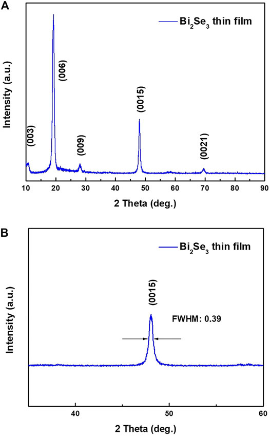
FIGURE 1. (A) XRD pattern of the Bi2Se3 single crystal film, (B) Zoomed in XRD pattern of the Bi2Se3 film at (0015) peak.
Figure 2 shows the X-ray photoelectron spectra (XPS) of Bi-4f and Se-3d of Bi2Se3 thin film. In the Bi-4f spectrum, two distinct peaks Bi-4f7/2 = 158.5 eV and Bi-4f5/2 = 164 eV are observed, both are intense and with binding energy. This is consistent with the Bi₂O₃ (Bi3+) phase, which leads to the conclusion that the Bi ions are in the tervalent state. Figure 2B reveals two adjacent sharp peaks in the Se-3d5/2 spectrum at 53.6 and 54.3 eV on 3d3/2 peaks, respectively. Compare with the X-ray Photoelectron Spectroscopy Database of the National Institute of Standards and Technology (NIST), and it can be inferred that the valence state of the Se ions is −2. XPS analysis reveals the valence states of Bi and Se to be +3 and −2 in the Bi2Se3 film, which is conducive to the formation of a pure Bi2Se3 phase. The atomic content of Bi and Se on the surface of the film is 0.47 and 0.53 respectively. The deviation of the surface stoichiometric ratio is due to the lower vapor pressure of the Se element, so Se is prone to volatilization during the growth process, especially on the surface of the film.
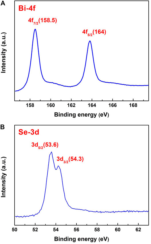
FIGURE 2. X-ray photoelectron spectra of Bi2Se3 thin film, (A) Bi-4f, (B) Se-3d.
Morphologies and Microstructure of the Bi2Se3 Film
Figure 3A shows the film’s surface morphology atomic force microscope (AFM) image. It shows that the nano-particles is uniform and arrange orderly with an average size of 120 nm. As shown in Figure 3B, a higher-magnification view of the surface revealed triangular crystal facets and terrace structures of the Bi2Se3 thin film. The root-mean-square (RMS) roughness value for the 2 μm × 2 μm area is 0.9 nm. The thickness of Bi2Se3 film is shown in Figure 3C. The image indicates that the Bi2Se3 film thickness is uniform and tightly bonded to the substrate. No lattice defects such as threading dislocations are observed at the interface. In Figure 3D, the interplanar d spacing between lattice fringes is measured to be 0.2 nm, in conformance with the d-spacing of the (11
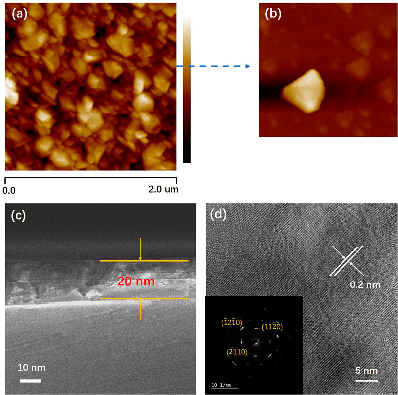
FIGURE 3. (A) 2 μm × 2 μm atomic force microscope images of the Bi2Se3 thin film, (B) Enlarged image of Bi2Se3 grain, (C) Cross-sectional SEM image of Bi2Se3 (001) thin film close to the interface of the substrate, (D) Surface HRTEM image and SAED pattern of Bi2Se3 thin film.
Optical Properties of Bi2Se3 Thin Film
Figure 4A gives the optical transmission spectrum of the Bi2Se3 film in visible light-near infrared band. All the measured data have been deducted from the influence of the substrate. The film exhibits a transmittance of 50–70% in the entire visible light band, and a higher transmittance of 70–85% in the near-infrared band. Figure 4B gives the absorption spectrum of Bi2Se3 thin film. At 3,000 nm wavelength stands a sharp absorption edge. It is the fundamental absorption which energy corresponds to the energy required for the electron to transition from the top of the valence band to the bottom of the conduction band. Therefore, this absorption edge has been widely adopted to determine the forbidden band width. The optical absorption coefficient (a) and photon energy (hv) has a relation as such:
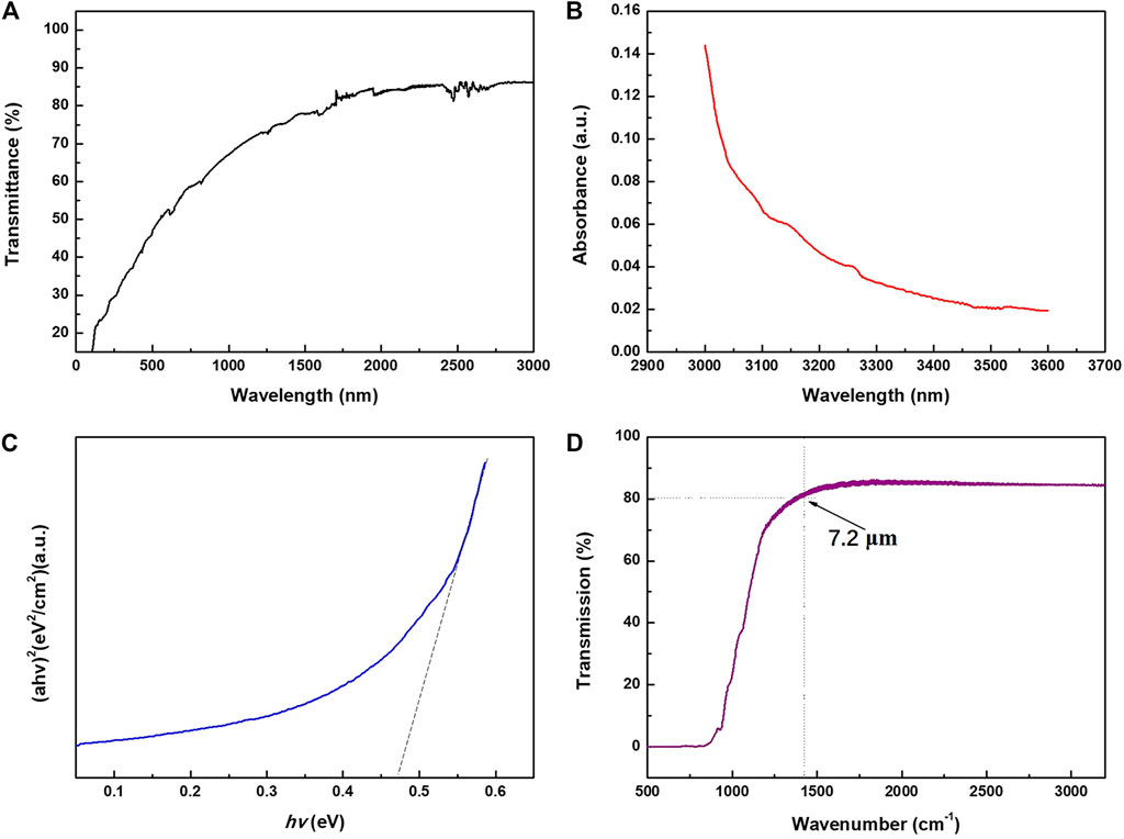
FIGURE 4. (A) Optical transmission spectrum of Bi2Se3 thin film, (B) Absorption spectrum of Bi2Se3 thin film, (C) (ahv)2 versus hv plot, and (D) Infrared transmission spectra of Bi2Se3 thin film.
Where Eg is the optical bandgap of the materials, A is a constant, and m hinges on the type of transition: m = 1/2 when band transition is indirect, and m = 2 when band transition is direct (Deng et al., 2013). Figure 4C delineates the linear relationship between (ahv)2 and hv, it indicates that the Bi2Se3 thin film has a direct bandgap structure. Extend the straight portion of the curve and the bandgap can be estimated as 0.47 eV. This value is a bit smaller than previously reported in the literature of 0.5 eV. Generally, the relationship between the forbidden band width and the carrier concentration can be expressed as such a linear relationship ΔE = ΔE (0) ‒ kn1/3, where n is carrier concentration. During the growth of Bi2Se3 thin film, high-temperature annealing will cause the absence of Se atoms, which will create Se vacancies in the film, forming a natural n-type semiconductor. The bulk carrier concentration n increases, so the actual measured band gap is lower than the theoretical value. Figure 4D shows the infrared transmission spectrum of the Bi2Se3 thin film. The total transmittance of Bi2Se3 film in the wavelength range of 3.2 (3,125 wavenumber) −7.2 (1,400 wavenumber) μm is as high as 85% with no obvious characteristic absorption peak. The high transmittance (or low absorptivity), especially in the infrared band, is primarily attributed to the free carrier plasma edge around the far-infrared frequency. Due to the collective oscillation of conduction band electrons, called plasma oscillation, the transmittance of the film decreases at 7.2 μm suddenly. According to Drude’s free electron theory, the plasma oscillation frequency ωp of the material determines the upper limit of the transmission wavelength. When the incident light frequency ω < ωp, the film exhibits strong reflectivity; when ω > ωp, the film exhibits transmittance. Thus, ωp sets the low cutoff frequency of the transmission band.
Electrical Characteristics of Bi2Se3 Thin Film
In order to further analyze the electrical characteristics and transmission characteristics of Bi2Se3 thin films. Multiple temperature Hall effect measurement were carried out for the low temperature range. The influences of temperature on the resistivity, carrier density and mobility were investigated. As well as high transmittance in infrared band, the Bi2Se3 thin film also exhibits excellent electrical properties. The graphics of temperature dependent carrier concentration, Hall mobility and resistivity are shown in Figures 5A–C. The electron concentration of the film increases as the temperature rises, and the bulk electron concentration of the film at room temperature is about 1.15×1017cm−3. The Hall mobility decreases as the temperature rises, and the Hall mobility at room temperature is as high as 1,015 cm2/Vs, which is two orders of magnitude higher than the copper-iron ore series p-type infrared transparent conductive film we prepared previously. The reason for the high mobility is that Bi2Se3 belongs to a three-dimensional topological insulator structure. The basic feature of the structure is that there are four time-reversed symmetry points in the Brillouin zone of its surface state with Kramers degenerate phenomenon, which form the Dirac Cone. The apex of the Dirac cone is called the Dirac point, and the dispersion relationship between energy and momentum near the apex is linear. Due to the spin-coupling effect, the spin direction of the surface state is always perpendicular to the direction of momentum, so that electrons travel on the surface with low loss (or lossless) at a speed similar to the photon. The Hall coefficient of Bi2Se3 film is −7.8 cm3C−1 at room temperature, which indicates characteristic of n-type conduction. The room temperature conductivity of the film is 7 × 10⁻⁴ Ωcm. As shown in Figure 5D, Bi2Se3 film shows thermal activation behavior at room temperature, because the plots of lnρ ∼1,000/T show a linear relation. The conductivity can be expressed by
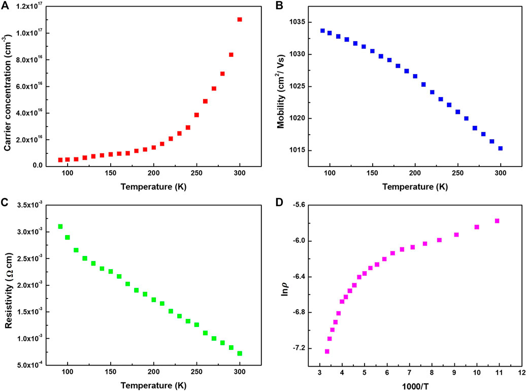
FIGURE 5. (A) Temperature dependence of: (A) Carrier concentration, (B) Hall mobility, (C) electrical resistivity (D) lnρ plotted as function of 1,000/T for the Bi2Se3 thin film.
Preparation and Measurement of Infrared Transparent Diode Device
In order demonstrate the application of our thin film, we made N-Bi2Se3/P-CuScO2 infrared transparent heterojunction diode, the schematic diagram of which is shown in Figure 6A. The schematic diagram of this diode is shown in Figure 6A. First, we use the polymer-assisted deposition method to grow the CuScO2 film with a thickness of about 200 nm on a sapphire substrate, and then deposit a layer of Bi2Se3 thin film with a thickness of 150 nm by MBE. Finally, we evaporate In on the surface of the device as the electrode. Figure 6B shows the I–V curve of the heterojunction diode. It can be easily found the rectifying characteristic through the curve, accompanied by a threshold voltage of 3.3 V, which is consistent with the forbidden band width of CuScO2 (3.3–3.5 eV). Thus, hetero-epitaxial growth at the CuScO2 (lower part) and Bi2Se3 (upper part) interface is demonstrated.
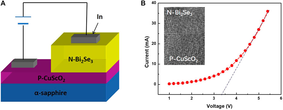
FIGURE 6. (A) Schematic structure of N-Bi2Se3/P-CuScO2 heterojunction diode device. (B) Current (I)—voltage (V) characteristics of N-Bi2Se3/P-CuScO2 diode device. The inset in (B) shows the cross-sectional HREM image of N-Bi2Se3/P-CuScO2 interface.
Conclusion
In this paper, we used molecular beam deposition (MBE) method to epitaxial grow Bi2Se3 thin film, which was then incorporated into N-Bi2Se3/P-CuScO2 infrared transparent heterojunction diodes. The unique growth and processing design of MBE underpins the high quality, epitaxial growth of the film. The Bi2Se3 thin film thus produced displayed remarkable optical transparency in IR region, and great n-type electrical conductivity. The CuScO2 film-based infrared transparent heterojunction diode has an abrupt interface, exhibits rectifying I—V characteristics with the threshold voltage of ∼3.3V. The results prove that the Bi2Se3 film has excellent optical and electrical properties in the wide-band infrared range. Such photoelectric properties make it a great candidate for window electrodes of infrared detectors, as well as other scenarios in the wide infrared wavelength range.
Data Availability Statement
The original contributions presented in the study are included in the article/Supplementary Material, further inquiries can be directed to the corresponding authors.
Author Contributions
All authors listed have made a substantial, direct, and intellectual contribution to the work and approved it for publication.
Conflict of Interest
The authors declare that the research was conducted in the absence of any commercial or financial relationships that could be construed as a potential conflict of interest.
Publisher’s Note
All claims expressed in this article are solely those of the authors and do not necessarily represent those of their affiliated organizations, or those of the publisher, the editors and the reviewers. Any product that may be evaluated in this article, or claim that may be made by its manufacturer, is not guaranteed or endorsed by the publisher.
Acknowledgments
Authors would like to express their gratitude to the Scientific Research Project of Jilin Provincial Department of Education (20190545KJ), National Natural Science Foundation of China (NSFC) (61905023); The Fourth Lifting Project of Young Science and Technology Talents in Jilin Province (QT202026); Natural Science Foundation of Jilin Province Science and Technology Department (20210101182JC).
References
Aydin, E., De Bastiani, M., Yang, X., Sajjad, M., Aljamaan, F., Smirnov, Y., et al. (2019). Zr‐Doped Indium Oxide (IZRO) Transparent Electrodes for Perovskite‐Based Tandem Solar Cells. Adv. Funct. Mater. 29, 1901741. doi:10.1002/adfm.201901741
Chen, T. c., Ma, T. p., and Barker, R. C. (1983). Infrared Transparent and Electrically Conductive Thin Film of In2O3. Appl. Phys. Lett. 43 (10), 901–903. doi:10.1063/1.94199
Chuai, Y.-H., Hu, B., Li, Y.-D., Shen, H.-Z., Zheng, C.-T., and Wang, Y.-D. (2015). Effect of Sn Substitution on the Structure, Morphology and Photoelectricity Properties of High C-axis Oriented CuFe1−xSnxO2 Thin Film. J. Alloys Compd. 627, 299–306. doi:10.1016/j.jallcom.2014.12.118
Chuai, Y.-H., Shen, H.-Z., Li, Y.-D., Hu, B., Zhang, Y., Zheng, C.-T., et al. (2015). Epitaxial Growth of Highly Infrared-Transparent and Conductive CuScO2 Thin Film by Polymer-Assisted-Deposition Method. RSC Adv. 5, 49301–49307. doi:10.1039/c5ra07743e
Chuai, Y.-H., Wang, X., Shen, H.-Z., Li, Y.-D., Zheng, C.-T., and Wang, Y.-D. (2016). Effects of Zn-Doping on Structure and Electrical Properties of P-type Conductive CuCr1−x Zn X O2 Delafossite Oxide. J. Mater. Sci. 51, 3592–3599. doi:10.1007/s10853-015-9679-4
Chuai, Y. H., Bai, Y., Zheng, C. T., Liu, C. Y., Wang, X., and Yue, D. (2019). Chemical Modulation of Valence Band and Photoelectric Properties of Epitaxial P-type Infrared Transparent Conducting CuScO2 Thin Films. Mater. Res. Express 6, 126460. doi:10.1088/2053-1591/ab78c8
Chuai, Y., Wang, X., Zheng, C., Zhang, Y., Shen, H., and Wang, Y. (2016). Highly Infrared-Transparent and P-type Conductive CuSc1−xSnxO2 Thin Films and a P-CuScO2:Sn/n-ZnO Heterojunction Fabricated by the Polymer-Assisted Deposition Method. RSC Adv. 6, 31726–31731. doi:10.1039/c6ra00919k
Deng, Z., Fang, X., Wu, S., Zhao, Y., Dong, W., Shao, J., et al. (2013). Structure and Optoelectronic Properties of Mg-Doped CuFeO2 Thin Films Prepared by Sol-Gel Method. J. Alloys Compd. 577, 658–662. doi:10.1016/j.jallcom.2013.06.155
Hasan, M. Z., and Kane, C. L. (2010). Colloquium: Topological Insulators. Rev. Mod. Phys. 82, 3045–3067. doi:10.1103/revmodphys.82.3045
Jain, P., Nakabayashi, Y., Haga, K.-i., and Tokumitsu, E. (2020). Electrical Properties of In2O3 and ITO Thin Films Formed by Solution Process Using In(acac)3 Precursors. Jpn. J. Appl. Phys. 59, SCCB12. doi:10.7567/1347-4065/ab4a89
Jash, A., Ghosh, S., Bharathi, A., and Banerjee, S. S. (2020). Coupling-decoupling of Conducting Topological Surface States in Thick Bi2Se3 Single Crystals. Phys. Rev. B 101, 165119. doi:10.1103/physrevb.101.165119
Johnson, L., and Moran, M. (2001). “Infrared Transparent Conductive Oxides,” in SPIE Proceedings,Window and Dome Technologies and Materials VII,289 4375.
Khan, A., Rahman, F., Nongjai, R., and Asokan, K. (2020). Structural, Optical and Electrical Transport Properties of Sn Doped In2O3. Solid State. Sci. 109, 106436. doi:10.1016/j.solidstatesciences.2020.106436
Lipkin, N., Zipin, H., Yadin, Y., Klein, Z., Dagan, L., and Marcovitch, O. (2001). “Dual Band Transparent Conductive Coating,” in Proc. SPIE 4375, Window and Dome Technologies and Materials VII, 315 4375. doi:10.1117/12.439190
Liu, F., Liu, M., Liu, A., Yang, C., Chen, C., Zhang, C., et al. (2015). The Effect of Temperature on Bi2Se3 Nanostructures Synthesized via Chemical Vapor Deposition. J. Mater. Sci. Mater. Electron. 26 (6), 3881–3886. doi:10.1007/s10854-015-2915-5
Park, J. Y., Lee, G.-H., Jo, J., Cheng, A. K., Yoon, H., Watanabe, K., et al. (2016). Molecular Beam Epitaxial Growth and Electronic Transport Properties of High Quality Topological Insulator Bi 2 Se 3 Thin Films on Hexagonal boron Nitride. 2d Mater. 3, 035029. doi:10.1088/2053-1583/3/3/035029
Qi, X.-L., and Zhang, S.-C. (2011). Topological Insulators and Superconductors. Rev. Mod. Phys. 83, 1057–1110. doi:10.1103/revmodphys.83.1057
Richardella, A., Zhang, D. M., Lee, J. S., Koser, A., Rench, D. W., Yeats, A. L., et al. (2010). Coherent Heteroepitaxy of Bi2Se3 on GaAs (111)B. Appl. Phys. Lett. 97, 262104. doi:10.1063/1.3532845
Sizov, F., Vuichyk, M., Svezhentsova, K., Tsybrii, Z., Stariy, S., and Smolii, M. (2021). CdTe Thin Films as Protective Surface Passivation to HgCdTe Layers for the IR and THz Detectors. Mater. Sci. Semiconductor Process. 124, 105577. doi:10.1016/j.mssp.2020.105577
Xia, Y., Qian, D., Hsieh, D., Wray, L., Pal, A., Lin, H., et al. (2009). Observation of a Large-gap Topological-Insulator Class with a Single Dirac Cone on the Surface. Nat. Phys 5 (6), 398–402. doi:10.1038/nphys1274
Yang, L., Han, J., Zhu, J., Zhu, Y., and Schlaberg, H. I. (2013). Chemical Bonding and Optoelectrical Properties of Ruthenium Doped Yttrium Oxide Thin Films. Mater. Res. Bull. 48, 4486–4490. doi:10.1016/j.materresbull.2013.07.039
Zhang, H., Liu, C.-X., Qi, X.-L., Dai, X., Fang, Z., and Zhang, S.-C. (2009). Topological Insulators in Bi2Se3, Bi2Te3 and Sb2Te3 with a Single Dirac Cone on the Surface. Nat. Phys 5 (6), 438–442. doi:10.1038/nphys1270
Zhang, L., Wang, B., Zhou, Y., Wang, C., Chen, X., and Zhang, H. (2020). Synthesis Techniques, Optoelectronic Properties, and Broadband Photodetection of Thin‐Film Black Phosphorus. Adv. Opt. Mater. 8, 2000045. doi:10.1002/adom.202000045
Keywords: thin film, Bi2Se3, optical property, electronic property, N-Bi2Se3/P-CuScO2 heterojunction
Citation: Chuai Y-H, Zhu C, Yue D and Bai Y (2022) Epitaxial Growth of Bi2Se3 Infrared Transparent Conductive Film and Heterojunction Diode by Molecular Beam Epitaxy. Front. Chem. 10:847972. doi: 10.3389/fchem.2022.847972
Received: 03 January 2022; Accepted: 10 January 2022;
Published: 25 January 2022.
Edited by:
Yue-Feng Liu, Jilin University, ChinaReviewed by:
Ziqi Yan, Shanghai Maritime University, ChinaZiying Wang, Hebei University of Technology, China
Copyright © 2022 Chuai, Zhu, Yue and Bai. This is an open-access article distributed under the terms of the Creative Commons Attribution License (CC BY). The use, distribution or reproduction in other forums is permitted, provided the original author(s) and the copyright owner(s) are credited and that the original publication in this journal is cited, in accordance with accepted academic practice. No use, distribution or reproduction is permitted which does not comply with these terms.
*Correspondence: Yu Bai, YmFpeXVAY3VzdC5lZHUuY24=