 Jia-Wei Tan1,2
 Gong Wang1,2*Guo-Xu Zhao1,2Ya-Chong Hou1,2De-Rong Sun1,2Yi-Fei Song1,2
 Le-Yan Dong1,2Hui Zhao3*Yulei Wang1,2
- 1Center for Advanced Laser Technology, Hebei University of Technology, Tianjin, China
- 2Hebei Key Laboratory of Advanced Laser Technology and Equipment, Tianjin, China
- 3School of Information and Electrical Engineering, Hebei University of Engineering, Handan, China
With high hardness, high thermal stability, chemical inertness and excellent optoelectronic properties, transparent hard and brittle materials have drawn significant attentions in frontier domains such as aerospace, photoelectric detection, and high-intensity lasers. Femtosecond laser processing technology demonstrates great potential for transparent hard and brittle materials processing due to its outstanding advantages such as non-contact, true 3D processing and programmable design. However, high-energy laser ablation usually causes severe damage to the surface of the materials, resulting in low processing accuracy, low processing efficiency and poor surface quality. Femtosecond laser hybrid processing strategies have been proven to be an effective solution to solve the above problems. This mini-review summarizes the fundamentals and research progress of femtosecond laser hybrid processing strategies of transparent hard and brittle materials in recent years. Moreover, the challenges and application prospects of these techniques are discussed.
Introduction
The rapid development of optoelectronics, nanophotonics, biomanufacturing and bionics has placed higher demands on the fabrication of micro/nanodevices. Transparent hard and brittle materials, such as diamond and sapphire, have become ideal choices for micro/nano devices operating under harsh environmental conditions such as strong radiation and easy corrosion, due to their high hardness, high thermal stability, chemical inertness, and broadband transparency (Khattak et al., 2016). However, its high hardness, high stability and other characteristics make it difficult to achieve precision processing by traditional processing techniques. For example, nano-embossing and thermal transfer technologies are not suitable for high hardness and high temperature-resistant materials, since the transfer process is easy to lead to the formation of chipping, cracking, and other stress damage. Femtosecond laser processing technology, as a new micro-nanofabrication tool, has shown great potential for micro-nano processing of transparent hard and brittle materials with the advantages of high processing accuracy, flexibility, contactless processing with no material selectivity (Chen et al., 2018; Sima et al., 2018; Lin and Hong, 2021). It enables flexible and efficient three-dimensional (3D) fabrication of submicron feature sizes and has a wide range of applications in the fabrication of 3D micro/nanostructures in the fields of micro-optics, micro-fluidics, super-impregnated functional surfaces, and bionic micro-robotics, which drives the development of functionalization, miniaturization, and integration of complex devices (Chen et al., 2012).
Tightly focused femtosecond laser has a high-power density. The sharp increase in temperature through electron collisions generated by inverse bremsstrahlung absorption and subsequent electron-lattice interactions leads to ablation and removal of material in and around the focused center of the spot. As a result, laser ablation has also become one of the most promising general laser processing technologies (Li et al., 2022; Liu S.-F et al., 2022). Femtosecond laser ablation techniques usually use a high power density above the material damage threshold to achieve material removal. Actually, material ablation removal is a non-equilibrium process. In the case of high-energy laser ablation, the ablated surface morphology changes. A large number of debris and particles are produced, which causes light scattering and hinders in subsequent process. The degree of damage to the material can be reduced by regulating the processing parameters. However, the inherent hardness, brittleness, and low light absorption of transparent hard and brittle materials make the processed surface quality and the processing efficiency still cannot meet the high requirements in micro-optics and microfluidics. Various femtosecond laser hybrid processing strategies have been proposed to address these challenges, providing many practical solutions for high-quality and high-precision processing of transparent hard and brittle materials.
In this mini-review, we summary the recent research advances in femtosecond laser hybrid processing strategies of transparent hard and brittle materials, focusing on three processing strategies: femtosecond laser-assisted etching strategy, liquid-assisted femtosecond laser ablation strategy, and femtosecond laser combined with annealing strategy. Moreover, this mini-review briefly discusses the challenges of femtosecond laser hybrid processing strategies and provides an outlook for the future.
Femtosecond laser-assisted etching strategy
Femtosecond laser-assisted etching strategy effectively improves the surface quality of transparent hard and brittle materials after femtosecond laser processing (Liu et al., 2019a). The basic principle is that the material is modified by femtosecond laser to induce a phase change or compositional change, which results in a different etching rate in the modified region and unmodified region. The modified areas can be removed during the subsequent etching process by controlling the etching parameters (Wang et al., 2022a). Ultimately, micro/nanostructures can be created on the surface or inside transparent hard and brittle materials. The etching process used is mainly divided into wet etching and dry etching.
Marcinkevičius et al. (2001) were the first to propose femtosecond laser-assisted wet etching and demonstrated direct 3D micromachining inside silica. It is worth noting that this technology allows the fabrication of 3D channels with diameters down to 10 mm in volume and with arbitrary interconnection angles and high aspect ratios. This pioneering work has demonstrated the feasibility of the strategy. However, the mechanism leading to the different etching rates is unclear. Researchers conducted extensive studies on the femtosecond laser-modified region and etching rate. For example, Bellouard et al. (2004) observed that the central portion of the laser processing path etched faster and explained the change in etching rate due to femtosecond laser modification. They suggest that the increase in etch rate is caused by two mechanisms: one by the presence of internal stresses and the other by a decrease in the average ring size of the structure due to changes in the crystalline state. This provides new insights into the laser-matter interaction. By ultra-high spatial resolution measurements, Hnatovsky et al. (2006) demonstrated that the difference in etching rates was dependent on the presence of polarization-dependent self-ordered periodic nanopores or nanopore structures. In addition, they investigated the optimal processing conditions for preparing high-quality microchannels, which had led to the development of 3D monolithic integration of microchannels and microphotonic assemblies. Mazilu et al. (2007) performed structural characterization of laser-modified regions inside sapphire. The results revealed the presence of dislocations near the sapphire crystal-amorphous boundary after femtosecond laser processing; while the high density of dislocations did not affect the etching ability of sapphire in aqueous hydrofluoric acid solutions. The luminescence and Raman characterization of the femtosecond laser-modified region were analyzed (Choudhury et al., 2013). It was demonstrated that femtosecond laser pulses transformed the neodymium-doped yttrium aluminum garnet (Nd:YAG) crystal state into a pre-damaged, which in turn showed a greater etching rate than that of the unmodified region.
The above-mentioned mechanistic studies lay a solid foundation for femtosecond laser-assisted wet etching to prepare micro/nanostructures. Self-organized nanostructures, elliptical microchannels and concave microstructures with smooth surfaces have been successfully prepared and applied in photonic crystals, biochemical analysis and super hydrophobicity (Wortmann et al., 2008; Hao et al., 2012; Bian et al., 2013). Shan et al. (2015) reported highly integrated on-chip 3D microcoil arrays inside fused silica, demonstrating the flexibility and versatility of femtosecond laser-assisted wet etching strategy. Wang et al. used temporally shaped femtosecond laser Bessel-beam-assisted chemical etching to achieve high throughput and high depth-to-diameter ratio microchannel preparation in fused silica (Wang et al., 2018). The etching depth was increased by 13 times with the temporally shaped Bessel beam modification compared with the conventional single pulse. In addition, Ródenas et al. (2019) demonstrated large-area 3D dense nanopore lattices prepared in yttrium aluminum garnet and sapphire crystals by wet etching-assisted laser direct writing techniques, respectively. They show that the wet etching rate can be increased by 5 orders of magnitude, making it possible to prepare arbitrary 3D structures with feature sizes of 100 nm.
In addition to processing micropore and microchannel structures (Juodkazis et al., 2008), microlens arrays (MLAs) of various shapes with good optical properties can be prepared by femtosecond laser-assisted wet etching strategy. As shown in Figure 1A, Chen et al. (2010) rapidly prepared large-area concave MLAs on quartz glass by this technique. Tightly stacked rectangular and hexagonal MLAs with diameters less than 100 μm were successfully fabricated in less than 3 h. Not only in planar transparent hard and brittle materials, femtosecond laser-assisted wet etching strategy also demonstrates flexibility in adjusting the shape and depth of structures. Du et al. (2012) prepared a honeycomb concave MLAs on a 3 mm diameter glass column. Hu et al. (2018) have successfully fabricated built-in microlenses in three-dimensional glass microfluidic channels. A wide range of continuous tuning by filling the channel with media with different refractive indices, which opens up new avenues for applications including biomedical imaging and sensing. Inspired by insect compound eyes, Wang et al. also successfully prepared glass infrared artificial compound eyes by this strategy. It has excellent infrared thermal imaging performance and a 60%–70% transmission rate (Wang et al., 2022b).
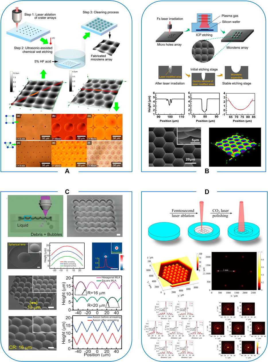
FIGURE 1. (A) Femtosecond laser-assisted wet etching; reproduced with permission from Chen et al. (2010). (B) Femtosecond laser-assisted dry etching; reproduced with permission from Liu et al. (2017). (C) Liquid-assisted femtosecond laser ablation; reproduced with permission from Hua et al. (2022). (D) Femtosecond laser combined with annealing; reproduced with permission from Schwarz et al. (2020).
Wet etching of crystalline materials is usually based on crystal orientation etching, which leads to distortion and pattern distortion of the structure (Deng et al., 2016). Therefore, it is not suitable for the preparation of high-quality bending devices. Dry etching technique is using the gas plasma to physically bombard and chemically react simultaneously with the etched material under the action of electric field in a low vacuum environment, which can avoid this problem to a large extent.
Liu et al. (2017) first proposed a dry etching-assisted femtosecond laser modification technique for processing hard materials, as shown in Figure 1B. They successfully prepared uniform, square and hexagonal MLAs with high-quality focusing and imaging capabilities on fused silica, gallium arsenide, silicon carbide, and diamond. This technology significantly improves processing efficiency (Liu et al., 2019b). More importantly, the technology is compatible with integrated circuit manufacturing processes and has significant application potential in the field of device integration. In addition, the technique enables the preparation of compound eye structures on curved sapphire. Compared with direct laser ablation, the processing efficiency of this technique can be improved by more than two orders of magnitude. Due to its high hardness and thermal stability, the sapphire concave compound eyes can be used as high-temperature and hard-cast templates.
To further solve the problem of difficulty in preparing deep structures, Zheng et al. (2021) achieved grating structures with adjustable period, duty cycle, and height on the sapphire surface by successively combining wet etching and dry etching processes assisted by femtosecond laser processing. The roughness of the sapphire grating structure was reduced from 78 nm (after laser direct writing) to 7 nm (after dry etching). Liu et al. realized the preparation of sapphire infrared windows with double-sided subwavelength pyramidal structure arrays using femtosecond laser-assisted etching strategy (Liu X.-Q et al., 2022). Notably, by introducing a sacrificial layer protection strategy, the competing problems of surface damage and internal damage during deep processing by inside-out femtosecond laser were solved. This provides a new idea for preparing transparent hard and brittle materials for micro/nanostructure preparation.
Liquid-assisted femtosecond laser ablation strategy
Liquid-assisted femtosecond laser ablation is another operative method to achieve high-precision true 3D processing of transparent hard and brittle materials. The femtosecond laser pulse is tightly focused at the intersection of material and liquid. The extremely high peak power of the laser focus causes the ablation of materials and pierces the liquid to produce laser cavitation. The shock wave generated by the expanding plasma plume and bubble collapse carries the ablated debris away from the surface, enabling real-time cleanup of debris during the ablation process. High-precision 3D processing of transparent hard and brittle materials is achieved through continuous controlled layer-by-layer material removal.
By comparing femtosecond laser processing in air and liquid, researchers found that liquid-assisted femtosecond laser ablation has better structural surface quality and higher processing resolution, with 1/3 to 1/2 reduction in ablation features (Cao et al., 2018). Sun et al. (2019) reported that liquid-assisted femtosecond laser processing reduced the ablation threshold of fused silica from 2.22 to 1.02 J/cm2. Since the femtosecond laser induces bubbles in the liquid after forming the plasma, different bubbles cause different impact pressures. Therefore, the ablation threshold reduction is closely related to the liquid with different properties. In addition, Wang et al. also prepared high-quality silicon carbide through-hole arrays without cracks and heat-affected zones by water-assisted femtosecond laser ablation technique, which is essential for the high-quality processing of silicon carbide electronic devices (Wang et al., 2021).
Liquid-assisted laser ablation can also reduce the thermal effects generated during laser processing. However, suspended debris and liquid flow can reduce the transmission stability of the femtosecond laser beam, resulting in less efficient energy transfer. For this reason, researchers proposed to process the back surface of materials to solve the above problem, i.e., laser-induced backside wet etching (LIBWE). This is the primary method for processing microstructures of transparent hard and brittle materials. Actually, LIBWE is mainly carried out through nanosecond laser pulses. Femtosecond laser pulses can easily lead to a liquid breakdown. However, considering the low heat affected zone, high resolution, and high surface quality, some studies still use femtosecond laser pulses. In this way, microstructures can be prepared in transparent hard and brittle materials with higher precision. For example, Ehrhardt et al. discovered two different laser-induced periodic surface structures (LIPSS) on SiO2 surfaces for the first time by LIBWE. This also provides additional data to discuss the origin of high spatial frequency LIPSS formation (Ehrhardt et al., 2018). Tan et al. (2019) successfully prepared 3D microchannels on glass by LIBWE. They used simultaneous spatial-temporal focusing to avoid the nonlinear self-focusing in the conventional focusing process. Seo et al. (2020) prepared glass microchannels using LIBWE. Based on this, combined with the laser-induced chemical liquid phase deposition method for rapid deposition of copper.
In addition, Hua et al. (2022) prepared different types of sapphire microlenses by cavitation-assisted femtosecond laser ablation technique. As shown in Figure 1C, the external profile of the prepared spherical microlenses is consistent with the theoretical design. Moreover, the further prepared square and hexagonal sapphire convex MLAs that can reach a fill factor of 100%, which is difficult to achieve by other techniques. This technique has also achieved the high-precision preparation of sapphire micro-optical components such as holographic diffraction elements, vortex light generators, and 3D artificial compound eyes.
Liquid-assisted laser ablation technology is based on an ablation processing mode and is suitable for any materials. The flow of the liquid eliminates the effect of debris during processing and reduces the thermal effects generated during processing. At the same time, the auxiliary cavitation kinetic process makes the machining more flexible and stable. However, achieving control of the process is complex, and the bubbles’ persistence, damage resistance, and mobility can simultaneously determine the final structural properties.
Femtosecond laser combined with annealing strategy
The annealing process is a traditional heat treatment technique. It can effectively eliminate the residual stress inside the material after laser processing and reduce the surface roughness of the material (Maia et al., 2021).
For glass materials, annealing of the laser-ablated structure allows the glass surface to start softening first. The softened surface produces a slight localized reflux under gravity and surface tension, resulting in a smoothness similar to a liquid surface. After cooling, the surface is again transformed into a glassy substance, while the surface quality is substantially improved. Seuthe et al. (2017) analyzed the structural relaxation of multi-component lithium silicate glass after femtosecond laser ablation combined with annealing using Raman spectroscopy. The results indicated that femtosecond laser-induced structural modifications were closely related to local changes in the refractive index of the materials. Subsequently, Sala et al. (2021) characterized the improvement in surface quality after thermal annealing, achieving a reduction in roughness from 49 nm to 19 nm. The reduction in roughness was demonstrated by the mirror imaging properties before and after thermal annealing. High-quality glass micro-optical elements were successfully prepared using the smoothing properties of this strategy (Lin et al., 2009; Wang et al., 2022). Compared with direct laser ablation, the annealing-assisted femtosecond laser processing technique can significantly improve processing efficiency and surface quality.
In addition, CO2 laser annealing also can be combined with femtosecond laser processing. The surface layer of the material is heated under the irradiation of a CO2 laser. Due to the surface tension of the material, the viscosity is reduced, thus improving the surface quality. Schwarz et al. (2018) prepared high-quality axicon for generating quasi-Bessel beams in fused silica by combining femtosecond laser ablation and CO2 laser polishing processes. This strategy provides the possibility for rapid prototyping of glass elements, even 3D optical elements with complex free-form surfaces. Microlens arrays with high profile accuracy and low roughness have also been successfully fabricated by this strategy (Figure 1D). It is also confirmed that femtosecond laser ablation combined with CO2 laser annealing is suitable for preparing complex optical geometry (Schwarz et al., 2020; Schwarz et al., 2021).
For crystal materials, laser ablation produces a rough amorphous layer. However, the main body of the structure remains in the single crystal state. By using a temperature higher than the softening point of the amorphous state and lower than the melting point of the crystal, it is possible to give the amorphous layer enough internal energy to soften and volatilize without changing the structure of the crystal body (He et al., 2013). Xu et al. (2013) prepared optical waveguides with low cladding and bilinear structure in LiTaO3 crystals using femtosecond laser ablation combined with annealing. After the thermal annealing process, the propagation loss of the cladding waveguide was reduced and its transmission loss was minimized to 0.38 dB/cm. He et al. (2016) observed grating regeneration during annealing and prepared a negative refractive index fiber Bragg grating with excellent performance. In addition, the stresses accumulated during laser processing can be eliminated by annealing treatment. Based on this, the crack-free 3D microstructure is also realized.
The thermal annealing process has become a common material treatment process. However, annealing temperature and time need to be strictly controlled for different materials. For example, too long an annealing time can lead to the deformation of glass body material. Structural deformation and surface quality need to be measured. For crystalline materials, the smoothing effect of annealing treatment on the material surface is relatively weak, requiring better surface preparation during laser processing.
Conclusion and outlook
We analyze the problems of low processing accuracy and poor structural surface quality as well as the severe damage to the material surface caused by femtosecond laser ablation technology. The research progresses of femtosecond laser hybrid processing strategies of transparent hard and brittle materials in recent years are reviewed. Hybrid processing strategies has become a new direction for micro-nano processing. For instance, femtosecond laser-assisted etching strategy can improve processing quality. However, as a point-by-point direct writing technology, the processing efficiency of femtosecond laser ablation can not meet the high requirements, and new auxiliary strategies need to be explored to improve the processing efficiency, such as parallel laser micro-nano processing technology. In addition, the combination of multiple technologies in order to achieve the integration of micro/nanodevices needs to be further investigated. In conclusion, femtosecond laser hybrid processing strategies play an increasingly significant role in the preparation and application of micro/nano devices for transparent hard and brittle materials. With the further exploration of femtosecond laser micro-nano processing technology, the preparation of micro/nano devices with arbitrary shape, low roughness and high resolution can be realized, which promote the development and accelerate the industrialization process of femtosecond laser micro-nano processing in aerospace, biomedical, information technology, new energy, new materials and other industries.
Author contributions
All authors listed have made a substantial, direct and intellectual contribution to the work, and approved it for publication.
Funding
This work was supported by the National Natural Science Foundation of China (Grant No. 62004059), Natural Science Foundation of Tianjin (20JCZDJC00430), Natural science research Foundation of Hebei University of Technology (JBKYXX2203), Natural Science Foundation of Hebei Province (Grant No. F2021202047), Funding Projects for the Introduction of Overseas Staff of Hebei Province (Grant No. C20210334), and Key Laboratory Fund Project (Grant No. 2021JCJQLB055004).
Conflict of interest
The authors declare that the research was conducted in the absence of any commercial or financial relationships that could be construed as a potential conflict of interest.
Publisher’s note
All claims expressed in this article are solely those of the authors and do not necessarily represent those of their affiliated organizations, or those of the publisher, the editors and the reviewers. Any product that may be evaluated in this article, or claim that may be made by its manufacturer, is not guaranteed or endorsed by the publisher.
References
Bellouard, Y., Said, A., Dugan, M., and Bado, P. (2004). Fabrication of high-aspect ratio, micro-fluidic channels and tunnels using femtosecond laser pulses and chemical etching. Opt. Express 12 (10), 2120–2129. doi:10.1364/OPEX.12.002120
Bian, H., Yang, H., Chen, F., Liu, H., Du, G., Deng, Z., et al. (2013). Scalable shape-controlled fabrication of curved microstructures using a femtosecond laser wet-etching process. Mater. Sci. Eng. C 33 (5), 2795–2799. doi:10.1016/j.msec.2013.02.048
Cao, X.-W., Chen, Q.-D., Fan, H., Zhang, L., Juodkazis, S., and Sun, H.-B. (2018). Liquid-assisted femtosecond laser precision-machining of silica. Nanomater. (Basel). 8 (5), 287. doi:10.3390/nano8050287
Chen, F., Liu, H.-W., Yang, Q., Wang, X.-H., Hou, C., Bian, H., et al. (2010). Maskless fabrication of concave microlens arrays on silica glasses by a femtosecond-laser-enhanced local wet etching method. Opt. Express 18 (19), 20334–20343. doi:10.1364/OE.18.020334
Chen, J., Liu, C.-S., Shang, S., Liu, D., Perrie, W., Dearden, G., et al. (2012). A review of ultrafast laser materials micromachining. Opt. Laser Technol. 46, 88–102. doi:10.1016/j.optlastec.2012.06.037
Chen, T.-H., Fardel, R., and Arnold, C. B. (2018). Ultrafast z-scanning for high-efficiency laser micro-machining. Light. Sci. Appl. 7, e17181. doi:10.1038/lsa.2017.181
Choudhury, D., Rodenas, A., Paterson, L., Diaz, F., Jaque, D., and Kar, A. K. (2013). Three-dimensional microstructuring of yttrium aluminum garnet crystals for laser active optofluidic applications. Appl. Phys. Lett. 103 (4), 041101. doi:10.1063/1.4816338
Deng, Z.-F., Chen, F., Yang, Q., Bian, H., Du, G.-Q., Yong, Y.-L., et al. (2016). Dragonfly-eye-inspired artificial compound eyes with sophisticated imaging. Adv. Funct. Mat. 26 (12), 1995–2001. doi:10.1002/adfm.201504941
Du, G., Yang, Q., Chen, F., Liu, H., Deng, Z., Bian, H., et al. (2012). Direct fabrication of seamless roller molds with gapless and shaped-controlled concave microlens arrays. Opt. Lett. 37 (21), 4404–4406. doi:10.1364/OL.37.004404
Ehrhardt, M., Lorenz, P., Han, B., Zhu, R., and Zimmer, K. (2018). Laser-induced backside wet etching of SiO2 with a visible ultrashort laser pulse by using KMnO4 solution as an absorber liquid. J. Laser Micro Nanoeng. 13 (2), 47–54. doi:10.2961/jlmn.2018.02.0001
Hao, B., Liu, H.-W., Chen, F., Yang, Q., Qu, P.-B., Du, G.-Q., et al. (2012). Versatile route to gapless microlens arrays using laser-tunable wet-etched curved surfaces. Opt. Express 20 (12), 12939–12948. doi:10.1364/OE.20.012939
He, R.-Y., An, Q., DeAldana, J. R. V., Lu, Q.-M., and Chen, F. (2013). Femtosecond-laser micromachined optical waveguides in Bi4Ge3O12 crystals. Appl. Opt. 52 (16), 3713–3718. doi:10.1364/AO.52.003713
He, J., Wang, Y.-P., Liao, C.-R., Wang, C., Liu, S., Yang, K.-M., et al. (2016). Negative-index gratings formed by femtosecond laser overexposure and thermal regeneration. Sci. Rep. 6, 23379. doi:10.1038/srep23379
Hnatovsky, C., Taylor, R. S., Simova, E., Rajeev, P. P., Rayner, D. M., Bhardwaj, V. R., et al. (2006). Fabrication of microchannels in glass using focused femtosecond laser radiation and selective chemical etching. Appl. Phys. A 84 (1-2), 47–61. doi:10.1007/s00339-006-3590-4
Hu, Y.-L., Rao, S.-L., Wu, S.-Z., Wei, P.-F., Qiu, W.-X., Wu, D., et al. (2018). All-glass 3D optofluidic microchip with built-in tunable microlens fabricated by femtosecond laser-assisted etching. Adv. Opt. Mat. 6 (9), 1701299. doi:10.1002/adom.201701299
Hua, J.-G., Liang, S.-Y., Chen, Q.-D., Juodkazis, S., and Sun, H.-B. (2022). Free-form micro-optics out of crystals: Femtosecond laser 3D sculpturing. Adv. Funct. Mat. 32 (26), 2200255. doi:10.1002/adfm.202200255
Juodkazis, S., Nishi, Y., and Misawa, H. (2008). Femtosecond laser-assisted formation of channels in sapphire using KOH solution. Phys. Stat. Sol. 2 (6), 275–277. doi:10.1002/pssr.200802203
Khattak, C. P., Shetty, R., Schwerdtfeger, C. R., and Ullal, S. (2016). World’s largest sapphire for many applications. J. Cryst. Growth 452, 44–48. doi:10.1016/j.jcrysgro.2015.11.026
Li, Z.-H., Hu, J., Jiang, L., Li, C., Liu, W., Liu, H.-L., et al. (2022). Shaped femtosecond laser-regulated deposition sites of galvanic replacement for simple preparation of large-area controllable noble metal nanoparticles. Appl. Surf. Sci. 579, 152123. doi:10.1016/j.apsusc.2021.152123
Lin, Z.-Y., and Hong, M.-H. (2021). Femtosecond laser precision engineering: From micron, submicron, to nanoscale. Ultrafast Sci. 3, 1–22. doi:10.34133/2021/9783514
Lin, C.-H., Jiang, L., Chai, Y.-H., Xiao, H., Chen, S.-J., and Tsai, H.-L. (2009). Fabrication of microlens arrays in photosensitive glass by femtosecond laser direct writing. Appl. Phys. A 97 (4), 751–757. doi:10.1007/s00339-009-5350-8
Liu, X.-Q., Chen, Q.-D., Guan, K.-M., Ma, Z.-C., Yu, Y.-H., Li, Q.-K., et al. (2017). Dry-etching-assisted femtosecond laser machining. Laser Phot. Rev. 11 (3), 1600115. doi:10.1002/lpor.201600115
Liu, X.-Q., Bai, B.-F., Chen, Q.-D., and Sun, H.-B. (2019a). Etching-assisted femtosecond laser modification of hard materials. Opto-electron. Adv. 2 (9), 19002101–19002114. doi:10.29026/oea.2019.190021
Liu, X.-Q., Yu, L., Yang, S.-N., Chen, Q.-D., Wang, L., Juodkazis, S., et al. (2019b). Optical nanofabrication of concave microlens arrays. Laser Phot. Rev. 13 (5), 1800272. doi:10.1002/lpor.201800272
Liu, S.-F., Hou, Z.-W., Lin, L.-H., Li, F., Zhao, Y., Li, X.-Z., et al. (2022). 3D nanoprinting of semiconductor quantum dots by photoexcitation-induced chemical bonding. Science 377 (6610), 1112–1116. doi:10.1126/science.abo5345
Liu, X.-Q., Zhang, Y.- L., Li, Q.- K., Zheng, J.-X., Lu, Y.-M., Juodkazis, S., et al. (2022). Biomimetic sapphire windows enabled by inside-out femtosecond laser deep-scribing. PhotoniX 3, 1. doi:10.1186/s43074-022-00047-3
Maia, J. M., Amorim, V. A., Viveiros, D., and Marques, P. V. S. (2021). Femtosecond laser micromachining of an optofluidics-based monolithic whispering-gallery mode resonator coupled to a suspended waveguide. Sci. Rep. 11 (1), 9128. doi:10.1038/s41598-021-88682-x
Marcinkevi lus, A., Juodkazis, S., Watanabe, M., Miwa, M., Matsuo, S., Misawa, H., et al. (2001). Femtosecond laser-assisted three-dimensional microfabrication in silica. Opt. Lett. 26 (5), 277–279. doi:10.1364/OL.26.000277
Mazilu, M., Juodkazis, S., Ebisui, T., Matsuo, S., and Misawa, H. (2007). Structural characterization of shock-affected sapphire. Appl. Phys. A 86 (2), 197–200. doi:10.1007/s00339-006-3732-8
Rodenas, A., Gu, M., Corrielli, G., Paie, P., John, S., Kar, A. K., et al. (2019). Three-dimensional femtosecond laser nanolithography of crystals. Nat. Photonics 13 (2), 105–109. doi:10.1038/s41566-018-0327-9
Sala, F., Paie, P., Vazquez, R. M., Osellame, R., and Bragheri, F. (2021). Effects of thermal annealing on femtosecond laser micromachined glass surfaces. Micromachines (Basel). 12 (2), 180. doi:10.3390/mi12020180
Schwarz, S., Rung, S., Esen, C., and Hellmann, R. (2018). Fabrication of a high-quality axicon by femtosecond laser ablation and CO2 laser polishing for quasi-Bessel beam generation. Opt. Express 26, 23287–23294. doi:10.1364/OE.26.023287
Schwarz, S., Rung, S., Esen, C., and Hellmann, R. (2020). Rapid fabrication of precise glass axicon arrays by an all laser-based manufacturing technology. J. Laser Appl. 32 (1), 012001. doi:10.2351/1.5134988
Schwarz, S., Götzendorfer, B., Rung, S., Esen, C., and Hellmann, R. (2021). Compact beam homogenizer module with laser-fabricated lens-arrays. Appl. Sci. (Basel). 11, 1018. doi:10.3390/app11031018
Seo, J. M., Kwon, K. K., Song, K. Y., Chu, C. N., and Ahn, S. H. (2020). Deposition of durable micro copper patterns into glass by combining laser-induced backside wet etching and laser-induced chemical liquid phase deposition methods. Materials 13 (13), 2977. doi:10.3390/ma13132977
Seuthe, T., Mermillod-Blondin, A., Grehn, M., Bonse, J., Wondraczek, L., and Eberstein, M. (2017). Structural relaxation phenomena in silicate glasses modified by irradiation with femtosecond laser pulses. Sci. Rep. 7, 43815. doi:10.1038/srep43815
Shan, C., Chen, F., Yang, Q., Li, Y.-Y., Bian, H., Yong, J.-L., et al. (2015). High-level integration of three-dimensional microcoils array in fused silica. Opt. Lett. 40 (17), 4050–4053. doi:10.1364/OL.40.004050
Sima, F., Sugioka, K., Vazquez, R. M., Osellame, R., Kelemen, L., and Ormos, P. (2018). Three-dimensional femtosecond laser processing for lab-on-a-chip applications. Nanophotonics 7 (3), 613–634. doi:10.1515/nanoph-2017-0097
Sun, X.-Y., Yu, J.-L., Hu, Y.-W., Cui, D.-M., Chen, G.-W., Chu, D.-K., et al. (2019). Study on ablation threshold of fused silica by liquid-assisted femtosecond laser processing. Appl. Opt. 58 (33), 9027–9032. doi:10.1364/AO.58.009027
Tan, Y.-X., Chu, W., Wang, P., Li, W.-B., Wang, Z., and Cheng, Y. (2019). Water-assisted laser drilling of high-aspect-ratio 3D microchannels in glass with spatiotemporally focused femtosecond laser pulses. Opt. Mat. Express 9 (4), 1971–1978. doi:10.1364/OME.9.001971
Wang, Z., Jiang, L., Li, X.-W., Wang, A.-D., Yao, Z.-L., Zhang, K.-H., et al. (2018). High-throughput microchannel fabrication in fused silica by temporally shaped femtosecond laser Bessel-beam-assisted chemical etching. Opt. Lett. 43 (1), 98–101. doi:10.1364/OL.43.000098
Wang, W.-J., Song, H.-W., Liao, K., and Mei, X, -S. (2021). Water-assisted femtosecond laser drilling of 4H-SiC to eliminate cracks and surface material shedding. Int. J. Adv. Manuf. Technol. 112 (1-2), 553–562. doi:10.1007/s00170-020-06262-1
Wang, S.-K., Zhang, F., Yang, Q., Li, M.-J., Hou, X., and Chen, F. (2022). Chalcogenide glass IR artificial compound eyes based on femtosecond laser microfabrication. Adv. Mat. Technol., 2200741. doi:10.1002/admt.202200741
Wang, B.-X., Qi, J.-Y., Lu, Y.-M., Zheng, J.-X., Xu, Y., and Liu, X.-Q. (2022a). Rapid fabrication of smooth micro-optical components on glass by etching-assisted femtosecond laser modification. Materials 15 (2), 678. doi:10.3390/ma15020678
Wang, B.-X., Zheng, J.-X., Qi, J.-Y., Guo, M.-R., Gao, B.-R., and Liu, X.-Q. (2022b). Integration of multifocal microlens array on silicon microcantilever via femtosecond-laser-assisted etching technology. Micromachines (Basel). 13 (2), 218. doi:10.3390/mi13020218
Wortmann, D., Gottmann, J., Brandt, N., and Horn-Solle, H. (2008). Micro- and nanostructures inside sapphire by fs-laser irradiation and selective etching. Opt. Express 16 (3), 1517–1522. doi:10.1364/OE.16.001517
Xu, M.-M., He, R.-Y., Sun, S.-Q., DeAldana, J. R. V., and Chen, F. (2013). Femtosecond laser micromachined optical waveguides in LiTaO3 crystal. Phys. Status Solidi RRL. 7 (11), 1014–1017. doi:10.1002/pssr.201308102
Keywords: femtosecond laser, 3D processing, micro-nano fabrication, transparent hard and brittle materials, hybrid processing strategy
Citation: Tan J-W, Wang G, Zhao G-X, Hou Y-C, Sun D-R, Song Y-F, Dong L-Y, Zhao H and Wang Y (2022) Femtosecond laser hybrid processing strategy of transparent hard and brittle materials. Front. Chem. 10:1082738. doi: 10.3389/fchem.2022.1082738
Received: 28 October 2022; Accepted: 14 November 2022;
Published: 24 November 2022.
Edited by:
Dongshi Zhang, Shanghai Jiao Tong University, ChinaReviewed by:
Xue-Qing Liu, Jilin University, ChinaJiangyou Long, Guangdong University of Technology, China
Copyright © 2022 Tan, Wang, Zhao, Hou, Sun, Song, Dong, Zhao and Wang. This is an open-access article distributed under the terms of the Creative Commons Attribution License (CC BY). The use, distribution or reproduction in other forums is permitted, provided the original author(s) and the copyright owner(s) are credited and that the original publication in this journal is cited, in accordance with accepted academic practice. No use, distribution or reproduction is permitted which does not comply with these terms.
*Correspondence: Gong Wang, d2FuZ2dvbmdAaGVidXQuZWR1LmNu; Hui Zhao, emhhb2h1aUBoZWJldS5lZHUuY24=