 Ali Deniz Özdemir
  Simon Kaiser
  Tobias Neumann 2
 Franz Symalla
  Wolfgang Wenzel
94% of researchers rate our articles as excellent or good
Learn more about the work of our research integrity team to safeguard the quality of each article we publish.
Find out more
ORIGINAL RESEARCH article
Front. Chem., 18 January 2022
Sec. Chemical Physics and Physical Chemistry
Volume 9 - 2021 | https://doi.org/10.3389/fchem.2021.809415
This article is part of the Research TopicDriving Innovation in Organic Optoelectronic Materials with Physics-based and Machine-learning De Novo MethodsView all 10 articles
Organic light emitting diodes (OLED) play an important role in commercial displays and are promising candidates for energy-efficient lighting applications. Although they have been continuously developed since their discovery in 1987, some unresolved challenges remain. The performance of OLEDs is determined by a multifaceted interplay of materials and device architectures. A commonly used technique to overcome the charge injection barrier from the electrodes to the organic layers, are doped injection layers. The optimization of doped injection layers is critical for high-efficiency OLED devices, but has been driven mainly by chemical intuition and experimental experience, slowing down the progress in this field. Therefore, computer-aided methods for material and device modeling are promising tools to accelerate the device development process. In this work, we studied the effect of doped hole injection layers on the injection barrier in dependence on material and layer properties by using a parametric kinetic Monte Carlo model. We were able to quantitatively elucidate the influence of doping concentration, material properties, and layer thickness on the injection barrier and device conductivity, leading to the conclusion that our kMC model is suitable for virtual device design.
Since their discovery in 1987 (Tang and VanSlyke, 1987) organic light emitting diodes (OLEDs) gained lots of attention in academia and industry and have been continuously developed. Modern OLEDs find application in display technology and are promising devices for efficient general lighting applications (Adachi et al., 2000; Forrest et al., 1997). Three major factors comprise the performance and usability of OLEDs: the internal quantum efficiency (IQE), the device driving voltage (Jou et al., 2015) and light outcoupling (Flämmich et al., 2011). Common strategies to improve OLED efficiency and lifetime are based on intuition and experimental trial-and-error approaches. Quantitative models of charge injection and transfer processes in OLEDs can help to systematically increase device performance and to overcome remaining issues (Lee et al., 2017; Friederich et al., 2019; Song et al., 2020). The enormous number of potential materials and device architectures turns the development of novel materials and devices into a time- and resource-intensive task. In recent years, multiscale computational methods successfully predicted charge carrier mobility in pure materials (Friederich et al., 2014; Massé et al., 2016; Kotadiya et al., 2018) and guest-host systems (Symalla et al., 2016), current voltage characteristics (Mesta et al., 2013; Kaiser et al., 2021) and photoluminescent quenching (Symalla et al., 2020b) thus gaining relevance for the organic electronics community to be used as a supporting tool in device development and optimization (Andrienko, 2018; Friederich et al., 2019). Established simulation methods to model charge transport, charge injection (extraction) in OLEDs are drift-diffusion methods (DD) (Rossi et al., 2020; Doan et al., 2019), macroscopic equivalent-circuit techniques (Nowy et al., 2010), and microscopic methods like kinetic Monte Carlo (kMC) or master equation approaches (ME) (Zojer, 2021). Despite their high computational costs, kMC based simulation methods emerge as a quantitative tool in device modeling (van der Holst et al., 2011; Symalla et al., 2018; Symalla et al., 2019). kMC simulations are capable of treating the charge hopping processes explicitly and to take into account electrostatic interactions with the surrounding charge carriers beyond a mean-field description (Casalegno et al., 2010; van der Holst et al., 2011; Casalegno et al., 2013; Liu et al., 2017). Another important advantage of kMC methods is the treatment of molecular doping where the coulomb interaction of charges located on neighboring molecular sites play a crucial role (Fediai et al., 2019; Fediai et al., 2020).
Doping of charge injection layers is an established technique to overcome obstacles like insufficient charge balance or limited charge carrier concentration in the device due to large charge injection barriers (Zhang and Blom, 2010; Chiba et al., 2017) and high driving voltages. However, understanding of these effects remains elusive. Therefore, we studied p-doping of hole injection layers (HIL) on the kMC level, focusing on: 1) the Fermi level alignment of the doped injection layer and 2) how the p-doping influences the conductivity of the device. Our results confirm that our kMC model is able to perform device and material simulations to systematically investigate the influence of doping concentration, material selection and layer thickness on Fermi level alignment and device conductivity.
We performed the simulations on systems represented by simple cubic latices (Bässler, 1993; Pasveer et al., 2005) for each organic layer with a lattice constant was d = 1 nm (Mesta et al., 2013). Electronic properties like the ionization potential (IP) of the host material, electron affinity (EA) of the dopants or energetic disorder were treated as parameters and could easily be replaced by data from first-principle calculations, as done in previous works (Friederich et al., 2016; Kaiser et al., 2021). Charge carrier transport, charge injection (ejection) and doping activation with the kMC package LightForge (LF) (Symalla et al., 2016). In this approach, each microscopic process inside the device is modeled as a discrete event, with a corresponding event-rate. Each lattice site i represents an organic molecule with predefined ionization potential
The injection of holes from the anode to molecular site i of the organic layers is considered as a discrete process modeled with the Miller-Abrahams (Miller and Abrahams, 1960) rate to account for the ability of the electrodes to dissipate continuous amounts of energy. The expression for the injection rate
where kBT is the thermal energy,
with electrode work function W, the electric field strength F and ri the distance between site i and the electrode projected onto the field direction. To take into account the Coulomb interaction between all charge carriers in the system, we consider the dynamic Coulomb contribution to the effective injection barrier:
where rij (rik) are the distances between the site i and all positive (negative) charges inside the device. After each kMC-step, the dynamic Coulomb interaction is recomputed by performing an Ewald-summation (Ewald, 1921). To fulfill the boundary condition of a constant electrostatic potential on the electrode surface, the screening term
We assume that charge carriers are localized on the individual sites and that the transport from site i to site j takes place as a hopping process with the Marcus rate (Marcus, 1956):
where Jij is the electronic coupling between the sites, λ the reorganization energy and ΔEij contains the difference of the site ionization potentials due to the energetic disorder, the applied electric field and the dynamic electrostatic potential like in Eq. 2. For the electronic coupling Jij we use the empiric expression:
where j0 is a constant, rij is the distance between site i and j and a0 is the coupling decay length. The values for j0 and a0 can be found in the supplementary information.
The doped HIL consists of host (H) and dopant (D) sites arranged in a cubic grid with the dopant sites randomly distributed in the lattice. For p-doping, the dopant extracts an electron from a host site, leading to an ionized host and negatively charged dopant molecule:
In the kMC protocol doping activation (ionization of a host/dopant pair) is treated by explicitly taking into account the Coulomb interaction VC of the host/dopant pair and the interaction between the host/dopant pair and all other charge carriers in the device (similar to ϕscreen discussed above). The doping activation energy reads:
where the first term
where rα(β)H(D) is the distance between the activated host (dopant) molecule and negative α (positive β) charge carriers inside the device. Since the dopants in the device are randomly distributed and charge carrier positions fluctuate strongly, ΔEext is a stochastic quantity and changes with each kMC step. We treat doping as charge transfer from the dopant to the host, with the doping activation rates obtained by using Equation 4 and replacing ΔEij by ΔEion.
In the first part of this study we investigated the effect of the doping concentration on the hole injection barrier between the anode and the doped HIL. The schematic structure of the simulated device is shown in Figure 1A. It consists of two organic layers where the first one is the doped HIL and the second one serves as hole blocking layer, with a layer thickness of 15 nm each. Both electrodes have the same workfunction W = 4.5 eV and no external voltage is applied. After activation of the host/dopant pairs free holes are ejected into the anode, leaving a negative net charge in the organic layer, causing an upwards shift of the energy levels. This process takes place until the tail states of the organic layer align with the Fermi level of the anode. Figure 1B shows the energy levels of the device after Fermi level alignment. As the energy barrier between the doped injection layer and insulating layer is constant, the Fermi level alignment causes a voltage drop in the insulating layer, which is observed in a slope of the energy levels. We compute the reduction of the injection barrier ΔEIB as the difference in average site energies of the first and last 1 nm–slice of the insulating layer.
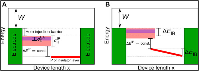
FIGURE 1. Schematic energy level diagram of the device to measure doping induced injection barrier reduction. The device consists of two identical electrodes with the workfunction W = 4.5 eV and two organic layers: the doped hole injection layer (HIL) and the hole blocking layer right to it. (A) The host ionization potential (IP)
Depending on the initial injection barrier, a low doping concentration may be sufficient to reach Fermi level alignment. Therefore, we studied ΔEIB in the insulating layer at different initial injection barriers and doping concentrations. This study was performed on the device displayed in Figure 1 at different doping concentrations and energy levels of the host and dopant sites. The difference between IP and EA was kept constant at 0.5 eV to ensure equal doping efficiencies between the simulations. The simulation was performed with λ = 0.2 eV for all three site types and
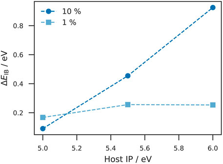
FIGURE 2. Injection barrier reduction at different host ionization potentials and doping concentrations. The reduction of the injection barrier ΔEIB is plotted against the host IP. The squares (dots) depict a doping concentration of 1% (10%). At a host IP of 5.0 eV, the observed ΔEIB for 10% doping concentration is smaller than for 1% which appears unexpected. However, this can be explained by considering the fact of a doping induced increase of the energetic disorder. For small initial injection barriers, the broadening of the energy levels leads to an overlap between the tail states and the electrode Fermi level, which in turn prevents further energy alignment. Nevertheless, the difference in ΔEIB is relatively small. For larger host IPs, ΔEIB remains almost constant at 1% doping concentration which can be explained by the fact that not enough dopants and thus free charge carriers are available to foster Fermi level alignment. At 10% doping concentration, we observe a significant increase in ΔEIB which is explained by the presence of sufficiently enough charge carriers.
Besides the doping concentration, we additionally investigated the effect of the layer thickness (with constant doping concentration) on the injection barrier. Figure 3 shows ΔEIB at different doping concentrations plotted against the layer thickness. At lower doping concentrations (1–3%), we observe how the layer thickness leads to a significant increase in ΔEIB. At a doping concentration of 1%, a high layer thickness leads to ΔEIB from 0.1 eV to almost 0.5 eV. With increasing doping concentration, this effect becomes steadily weaker to the point where it becomes negligible: at 7 and 10% the voltage drop does not increase with the layer thickness. At a layer thickness of 15 nm, we observe a voltage drop of about 0.5 eV for all doping concentrations, with a clearly visible offset especially between the 10% curve and the others. An explanation for the offset could be the finite size effect: the site energy levels are Gaussian distributed so that the probability for host sites with tail-state energies is lower for high doping concentrations. Thus, if the tail-states are truncated, a higher energy shift is required to achieve Fermi level alignment which results in larger voltage drops in the order of the energetic disorder. These results imply, that the tendency of the doped injection layer to align with Fermi level depends on the number of intrinsically free charge carriers and thus on the number of dopants present. To increase the number of free charge carriers, there are two possibilities: increasing 1) doping concentration or 2) the layer thickness of the doped HIL.
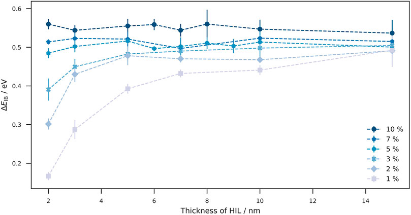
FIGURE 3. Effect of layer thickness on the ΔEIB. At a given doping concentration, the thickness of the doped injection layer controls ΔEIB. While the effect of layer thickness is significant at low concentrations (1–3%), ΔEIB at large doping concentration remains almost constant with increasing layer thickness. The weak variation of ΔEIB at doping concentrations of 5–10% is due to the fact that sufficient dopants are already present at low layer thicknesses to provide enough charge carriers for Fermi-level alignment. A direct implication of the dependence of ΔEIB on the total number of dopants is that, in addition to the doping concentration, the layer thickness of the doped injection layer can also be considered as a parameter for the reduction of the injection barrier. At maximum layer thickness, ΔEIB converges to a value of about 0.5 eV, with an offset between the doping concentrations.
In the second part of this work, we investigated how doped injection layers affect the transport properties in OLED devices. For this purpose we use a modified device with the hole blocking layer replaced by a hole transport layer (HTL) with the same energy levels as the host material in the doped HIL and a small energetic disorder of
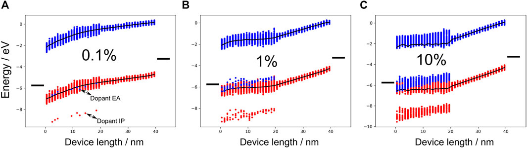
FIGURE 4. Energy diagrams of the test device for conductivity simulations. The black bars on the left of each panel represents the Fermi level of the electrodes. The red and blue dots illustrate the IP and EA, respectively. With a doping concentration of 0.1% (A), the majority of red (blue) dots represent the host IPs (EAs). The dopant IPs and EAs are explicitly annotated. At such small doping concentrations, no Fermi level alignment is achieved. With a doping concentration of 1% (B), the injection barrier is significantly smaller compared to the low doping case. Fermi level alignment is accomplished at a large doping concentration of 10% (C).
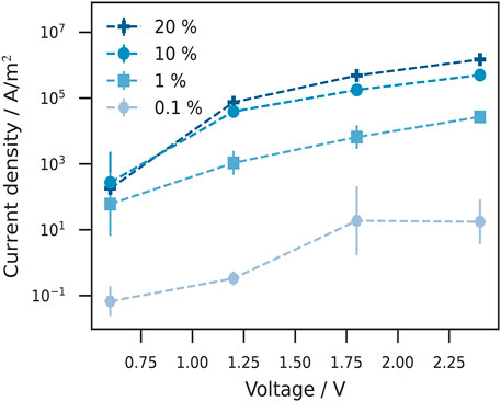
FIGURE 5. Current voltage characteristics (J–V-curve) at different doping concentrations. The current density is plotted against the applied voltage. At a low doping concentration 0.1% the current density is significantly smaller than for 1% doping concentration. Higher doping concentrations (10%) lead to an further increase of the current density. The difference between the 10 and 20% JV-curves is relatively small, suggesting saturation of the doping effect on the conductivity. The results here are in line with the energy diagrams in Figure 4.
We have already discussed that Fermi level alignment can also be achieved for host materials that have a large IP when the doping concentration is sufficiently high (see Figure 2). The impact on device conductivity has an even greater importance for practical work, which is why the relationship between the current density, ionization potential of the host material and doping concentration was investigated here. For a given electrode workfunction, the host IP determines the initial hole injection barrier, before Fermi level alignment takes place due host/dopant ionization. In Figure 6, the current density is plotted against the doping concentration at different host IPs. At a low doping concentration (0.1%), the current density for host materials with smaller IP (
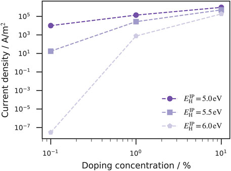
FIGURE 6. Current density as a function of the doping concentration and host ionization potentials (IP). The relation between the IP of the host materials and the anode workfunction determine the initial hole injection barrier. At small doping concentrations (0.1%) the current density for the host material with
Doping of charge injection layers is an important step to control and improve overall OLED device performance. Computer-aided methods, such as the kMC model introduced here can accelerate the search for ideal host/dopant pairs and optimal device architecture. kMC methods struggle in modelling doped injection layers, because the computational effort scales badly with the number of carriers. Doped injection layers have a large number of carriers, leading to many fast processes due to the high conductivity in efficiently doped materials. For the simulation of realistic multi-layer OLEDs, most of the kMC steps are required for the doped injection layer, rendering explicit kMC simulations of full-stack devices numerically unfeasible. One way to overcome this problem is to treat doped injection layers as an effective electrode. However, this approximation is not suitable for accurate simulations of the current density, which we have shown in Supplementary Figure S1. Here we report on kMC simulations of the doped hole injection layer in a cubic, two-layer device that enable us to investigate the performance of the injection layer as a function of the doping concentration, the ionization potential of the host material, and the thickness of the layer.
One particular important aspect is the effect of doping the injection layer and the injection barrier on Fermi level alignment. Using the device shown in Figure 1 we could vary a wide range of critical parameters, such as host IP or dopant concentration to provide insights into the interplay of materials and layer configurations. In fabricated devices, the injection barrier is determined by the selection of the host material. Even with this parameter predetermined, this simulation can help optimize the doping concentration for Fermi level alignment and charge balance in the emissive layer.
Our results show that our kMC model is conceptually well suited to study the influence of doped injection layers on the device properties. We have shown in Figure 2 that by increasing the doping concentration, Fermi level alignment can be achieved even with large host IPs. In addition, we observed that a large layer thickness (with constant doping concentration) fosters Fermi level alignment. The effect of doping on current density is of particular practical interest. We could demonstrate that increasing the doping concentration can cause the current density to increase by many orders of magnitude (see Figure 5).
The simulated systems can be extended from cubic to realistic structures (Neumann et al., 2013), but we note that this approximation is less severe than one might think, because the off-diagonal disorder is captured by the distribution of hopping matrix elements. When applied to novel materials, accurate EAs and IPs can be obtained using ab-initio calculations (Armleder et al., 2021) and the Coulomb interaction of host/dopant pairs can be computed quantum-mechanically (Symalla et al., 2020a). In combination with an ab-initio parametrization, this work can help to accelerate computational screening for ideal host/dopant materials in doped injection layers and optimization of material composition and layer arrangements. In crystalline organic semiconductors the description of charge transport as sequential hopping processes may be invalidated by delocalization effects, which can occur especially at high doping concentrations or materials with high mobilities (Troisi, 2011; Oberhofer et al., 2017). Mixed quantum-classical methods (Wang et al., 2015; Stafström, 2010) might be used to take into account these effects.
In order to make kMC simulations of realistic many-layer OLEDs feasible, it is necessary to treat the doped injections layer in a special way. Treating the doped injection layer as an effective anode is thus not a general solution to the problem of kMC models when simulating entire OLED stacks, so more sophisticated effective models of the doped injection layer may solve the simulation time issue more precisely.
The raw data supporting the conclusions of this article will be made available by the authors, without undue reservation.
AÖ and SK contributed equally to this work. SK, TN, FS, and WW conceived the idea and planned the theoretical calculations; SK, FS wrote and improved simulation software for this work; SK, AÖ carried out the simulations; and AÖ, SK prepared the manuscript with the inputs from all the co-authors and substantial revision from WW.
AÖ received funding by GRK 2450 “Scale bridging methods in computational nanoscience.” SK received funding by the High-Performance Computing 2 program of the Baden-Württemberg Stiftung (Project MSMEE). WW acknowledges funding by the Deutsche Forschungsgemeinschaft (DFG) in the Research and Training Program “Tailored Scale Bridging Approaches to Computational Nanoscience” and under Germany’s Excellence Strategy — 2082/1 — 390 761 711 (3DMM2O).
Authors TN and FS were employed by the company Nanomatch GmbH.
The remaining authors declare that the research was conducted in the absence of any commercial or financial relationships that could be construed as a potential conflict of interest.
All claims expressed in this article are solely those of the authors and do not necessarily represent those of their affiliated organizations, or those of the publisher, the editors and the reviewers. Any product that may be evaluated in this article, or claim that may be made by its manufacturer, is not guaranteed or endorsed by the publisher.
The Supplementary Material for this article can be found online at: https://www.frontiersin.org/articles/10.3389/fchem.2021.809415/full#supplementary-material
Adachi, C., Baldo, M. A., Forrest, S. R., and Thompson, M. E. (2000). High-efficiency Organic Electrophosphorescent Devices with Tris(2-Phenylpyridine)iridium Doped into Electron-Transporting Materials. Appl. Phys. Lett. 77, 904–906. doi:10.1063/1.1306639
Andrienko, D. (2018). “Multiscale Concepts in Simulations of Organic Semiconductors,” in Handbook of Materials Modeling. Editors W. Andreoni, and S. Yip (Cham: Springer International Publishing), 1–12. doi:10.1007/978-3-319-42913-7_39-1
Arkhipov, V. I., Heremans, P., Emelianova, E. V., and Bässler, H. (2005). Effect of Doping on the Density-Of-States Distribution and Carrier Hopping in Disordered Organic Semiconductors. Phys. Rev. B 71, 045214. doi:10.1103/PhysRevB.71.045214
Armleder, J., Strunk, T., Symalla, F., Friederich, P., Enrique Olivares Peña, J., Neumann, T., et al. (2021). Computing Charging and Polarization Energies of Small Organic Molecules Embedded into Amorphous Materials with Quantum Accuracy. J. Chem. Theor. Comput. 17, 3727–3738. doi:10.1021/acs.jctc.1c00036
Aydin, G., and Yavuz, I. (2021). Intrinsic Static/Dynamic Energetic Disorders of Amorphous Organic Semiconductors: Microscopic Simulations and Device Study. J. Phys. Chem. C 125, 6862–6869. doi:10.1021/acs.jpcc.0c11219
Bässler, H. (1993). Charge Transport in Disordered Organic Photoconductors a Monte Carlo Simulation Study. Phys. Stat. Sol. (B) 175, 15–56. doi:10.1002/pssb.2221750102
Casalegno, M., Bernardi, A., and Raos, G. (2013). Numerical Simulation of Photocurrent Generation in Bilayer Organic Solar Cells: Comparison of Master Equation and Kinetic Monte Carlo Approaches. J. Chem. Phys. 139, 024706. doi:10.1063/1.4812826
Casalegno, M., Raos, G., and Po, R. (2010). Methodological Assessment of Kinetic Monte Carlo Simulations of Organic Photovoltaic Devices: The Treatment of Electrostatic Interactions. J. Chem. Phys. 132, 094705. doi:10.1063/1.3337909
Chiba, T., Pu, Y.-J., Ide, T., Ohisa, S., Fukuda, H., Hikichi, T., et al. (2017). Addition of Lithium 8-Quinolate into Polyethylenimine Electron-Injection Layer in OLEDs: Not Only Reducing Driving Voltage but Also Improving Device Lifetime. ACS Appl. Mater. Inter. 9, 18113–18119. doi:10.1021/acsami.7b02658
Doan, D.-H., Glitzky, A., and Liero, M. (2019). Analysis of a Drift-Diffusion Model for Organic Semiconductor Devices. Z. Angew. Math. Phys. 70, 55. doi:10.1007/s00033-019-1089-z
Ewald, P. P. (1921). Die Berechnung optischer und elektrostatischer Gitterpotentiale. Ann. Phys. 369, 253–287. doi:10.1002/andp.19213690304
Fediai, A., Emering, A., Symalla, F., and Wenzel, W. (2020). Disorder-driven Doping Activation in Organic Semiconductors. Phys. Chem. Chem. Phys. 22, 10256–10264. doi:10.1039/D0CP01333A
Fediai, A., Symalla, F., Friederich, P., and Wenzel, W. (2019). Disorder Compensation Controls Doping Efficiency in Organic Semiconductors. Nat. Commun. 10, 4547. doi:10.1038/s41467-019-12526-6
Flämmich, M., Frischeisen, J., Setz, D. S., Michaelis, D., Krummacher, B. C., Schmidt, T. D., et al. (2011). Oriented Phosphorescent Emitters Boost OLED Efficiency. Org. Electronics 12, 1663–1668. doi:10.1016/j.orgel.2011.06.011
Forrest, S. R., Burrows, P. E., Shen, Z., Gu, G., Bulovic, V., and Thompson, M. E. (1997). The Stacked OLED (SOLED): a New Type of Organic Device for Achieving High-Resolution Full-Color Displays. Synth. Met. 91, 9–13. doi:10.1016/S0379-6779(97)03966-0
Friederich, P., Fediai, A., Kaiser, S., Konrad, M., Jung, N., and Wenzel, W. (2019). Toward Design of Novel Materials for Organic Electronics. Adv. Mater. 31, 1808256. doi:10.1002/adma.201808256
Friederich, P., Meded, V., Poschlad, A., Neumann, T., Rodin, V., Stehr, V., et al. (2016). Molecular Origin of the Charge Carrier Mobility in Small Molecule Organic Semiconductors. Adv. Funct. Mater. 26, 5757–5763. doi:10.1002/adfm.201601807
Friederich, P., Symalla, F., Meded, V., Neumann, T., and Wenzel, W. (2014). Ab Initio Treatment of Disorder Effects in Amorphous Organic Materials: Toward Parameter Free Materials Simulation. J. Chem. Theor. Comput. 10, 3720–3725. doi:10.1021/ct500418f
Jou, J.-H., Kumar, S., Agrawal, A., Li, T.-H., and Sahoo, S. (2015). Approaches for Fabricating High Efficiency Organic Light Emitting Diodes. J. Mater. Chem. C 3, 2974–3002. doi:10.1039/C4TC02495H
Kaiser, S., Kotadiya, N. B., Rohloff, R., Fediai, A., Symalla, F., Neumann, T., et al. (2021). De Novo Simulation of Charge Transport through Organic Single-Carrier Devices. J. Chem. Theor. Comput. 17, 6416–6422. doi:10.1021/acs.jctc.1c00584
Kotadiya, N. B., Mondal, A., Xiong, S., Blom, P. W. M., Andrienko, D., and Wetzelaer, G. J. A. H. (2018). Rigorous Characterization and Predictive Modeling of Hole Transport in Amorphous Organic Semiconductors. Adv. Electron. Mater. 4, 1800366. doi:10.1002/aelm.201800366
Lee, S.-M., Kwon, J. H., Kwon, S., and Choi, K. C. (2017). A Review of Flexible OLEDs toward Highly Durable Unusual Displays. IEEE Trans. Electron. Devices 64, 1922–1931. Conference Name: IEEE Transactions on Electron Devices. doi:10.1109/TED.2017.2647964
Liu, F., van Eersel, H., Xu, B., Wilbers, J. G. E., de Jong, M. P., van der Wiel, W. G., et al. (2017). Effect of Coulomb Correlation on Charge Transport in Disordered Organic Semiconductors. Phys. Rev. B 96, 205203. doi:10.1103/PhysRevB.96.205203
Marcus, R. A. (1956). On the Theory of Oxidation‐Reduction Reactions Involving Electron Transfer. I. J. Chem. Phys. 24, 966–978. doi:10.1063/1.1742723
Massé, A., Friederich, P., Symalla, F., Liu, F., Nitsche, R., Coehoorn, R., et al. (2016). Ab Initiocharge-Carrier Mobility Model for Amorphous Molecular Semiconductors. Phys. Rev. B 93, 195209. doi:10.1103/PhysRevB.93.195209
Mesta, M., Carvelli, M., de Vries, R. J., van Eersel, H., van der Holst, J. J. M., Schober, M., et al. (2013). Molecular-scale Simulation of Electroluminescence in a Multilayer white Organic Light-Emitting Diode. Nat. Mater 12, 652–658. doi:10.1038/nmat3622
Miller, A., and Abrahams, E. (1960). Impurity Conduction at Low Concentrations. Phys. Rev. 120, 745–755. doi:10.1103/PhysRev.120.745
Neumann, T., Danilov, D., Lennartz, C., and Wenzel, W. (2013). Modeling Disordered Morphologies in Organic Semiconductors. J. Comput. Chem. 34, 2716–2725. doi:10.1002/jcc.23445
Nowy, S., Ren, W., Elschner, A., Lövenich, W., and Brütting, W. (2010). Impedance Spectroscopy as a Probe for the Degradation of Organic Light-Emitting Diodes. J. Appl. Phys. 107, 054501. doi:10.1063/1.3294642
Oberhofer, H., Reuter, K., and Blumberger, J. (2017). Charge Transport in Molecular Materials: An Assessment of Computational Methods. Chem. Rev. 117, 10319–10357. doi:10.1021/acs.chemrev.7b00086
Pasveer, W. F., Cottaar, J., Tanase, C., Coehoorn, R., Bobbert, P. A., Blom, P. W. M., et al. (2005). Unified Description of Charge-Carrier Mobilities in Disordered Semiconducting Polymers. Phys. Rev. Lett. 94, 206601. doi:10.1103/PhysRevLett.94.206601
Rossi, D., Palazzo, D., Di Carlo, A., and Auf der Maur, M. (2020). Drift‐Diffusion Study of the IQE Roll‐Off in Blue Thermally Activated Delayed Fluorescence OLEDs. Adv. Electron. Mater. 6, 2000245. doi:10.1002/aelm.202000245
Song, J., Lee, H., Jeong, E. G., Choi, K. C., and Yoo, S. (2020). Organic Light‐Emitting Diodes: Pushing toward the Limits and beyond. Adv. Mater. 32, 1907539. doi:10.1002/adma.201907539
Stafström, S. (2010). Electron Localization and the Transition from Adiabatic to Nonadiabatic Charge Transport in Organic Conductors. Chem. Soc. Rev. 39, 2484. doi:10.1039/b909058b
Symalla, F., Fediai, A., Armleder, J., Kaiser, S., Strunk, T., Neumann, T., et al. (2020a). 43‐3: Ab‐initio Simulation of Doped Injection Layers. SID Symp. Dig. Tech. Pap. 51, 630–633. doi:10.1002/sdtp.13946
Symalla, F., Friederich, P., Kaiser, S., Strunk, T., Neumann, T., and Wenzel, W. (2018). 26-4: Computer-Aided Optimization of Multilayer OLED Devices. SID Symp. Dig. Tech. Pap. 49, 340–342. doi:10.1002/sdtp.12556
Symalla, F., Friederich, P., Massé, A., Meded, V., Coehoorn, R., Bobbert, P., et al. (2016). Charge Transport by Superexchange in Molecular Host-Guest Systems. Phys. Rev. Lett. 117, 276803. doi:10.1103/PhysRevLett.117.276803
Symalla, F., Heidrich, S., Friederich, P., Strunk, T., Neumann, T., Minami, D., et al. (2020b). Multiscale Simulation of Photoluminescence Quenching in Phosphorescent OLED Materials. Adv. Theor. Simul. 3, 1900222. doi:10.1002/adts.201900222
Symalla, F., Heidrich, S., Kubillus, M., Strunk, T., Neumann, T., and Wenzel, W. (2019). 19‐4: Boosting OLED Performance with Ab‐initio Modeling of Roll‐off and Quenching Processes. SID Symp. Dig. Tech. Pap. 50, 259–262. doi:10.1002/sdtp.12905
Tang, C. W., and VanSlyke, S. A. (1987). Organic Electroluminescent Diodes. Appl. Phys. Lett. 51, 913–915. doi:10.1063/1.98799
Troisi, A. (2011). Charge Transport in High Mobility Molecular Semiconductors: Classical Models and New Theories. Chem. Soc. Rev. 40, 2347–2358. doi:10.1039/C0CS00198H
van der Holst, J. J. M., van Oost, F. W. A., Coehoorn, R., and Bobbert, P. A. (2011). Monte Carlo Study of Charge Transport in Organic sandwich-type Single-Carrier Devices: Effects of Coulomb Interactions. Phys. Rev. B 83, 085206. doi:10.1103/PhysRevB.83.085206
Wang, L., Prezhdo, O. V., and Beljonne, D. (2015). Mixed Quantum-Classical Dynamics for Charge Transport in Organics. Phys. Chem. Chem. Phys. 17, 12395–12406. doi:10.1039/C5CP00485C
Zhang, Y., and Blom, P. W. M. (2010). Enhancement of the Hole Injection into Regioregular Poly(3-Hexylthiophene) by Molecular Doping. Appl. Phys. Lett. 97, 083303. doi:10.1063/1.3464560
Keywords: OLED, KMC, organic semiconductor, hole injection layer, doping
Citation: Özdemir AD, Kaiser S, Neumann T, Symalla F and Wenzel W (2022) Systematic kMC Study of Doped Hole Injection Layers in Organic Electronics. Front. Chem. 9:809415. doi: 10.3389/fchem.2021.809415
Received: 05 November 2021; Accepted: 13 December 2021;
Published: 18 January 2022.
Edited by:
Paul Winget, Schrodinger, United StatesReviewed by:
Bronson Philippa, James Cook University, AustraliaCopyright © 2022 Özdemir , Kaiser , Neumann , Symalla and Wenzel . This is an open-access article distributed under the terms of the Creative Commons Attribution License (CC BY). The use, distribution or reproduction in other forums is permitted, provided the original author(s) and the copyright owner(s) are credited and that the original publication in this journal is cited, in accordance with accepted academic practice. No use, distribution or reproduction is permitted which does not comply with these terms.
*Correspondence: Wolfgang Wenzel , d29sZmdhbmcud2VuemVsQGtpdC5lZHU=
†These authors share first authorship
Disclaimer: All claims expressed in this article are solely those of the authors and do not necessarily represent those of their affiliated organizations, or those of the publisher, the editors and the reviewers. Any product that may be evaluated in this article or claim that may be made by its manufacturer is not guaranteed or endorsed by the publisher.
Research integrity at Frontiers
Learn more about the work of our research integrity team to safeguard the quality of each article we publish.