 Razvan Krause1,2*
 Mariana Chávez-Cervantes2Sven Aeschlimann1,2
 Stiven Forti3Filippo Fabbri3,4,5
 Antonio Rossi3,4
 Camilla Coletti3,5Cephise Cacho6
 Yu Zhang7
 Paulina Ewa Majchrzak8Richard T. Chapman7Emma Springate7
 Isabella Gierz1*
- 1Institute for Experimental and Applied Physics, University of Regensburg, Regensburg, Germany
- 2Max Planck Institute for the Structure and Dynamics of Matter, Center for Free Electron Laser Science, Hamburg, Germany
- 3Center for Nanotechnology Innovation at IIT@NEST, Istituto Italiano di Tecnologia, Pisa, Italy
- 4National Enterprise for nanoScience and nanoTechnology (NEST), Istituto Nanoscienze, Consiglio Nazionale delle Ricerche (CNR) and Scuola Normale Superiore, Pisa, Italy
- 5Graphene Labs, Istituto Italiano di Tecnologia, Genova, Italy
- 6Diamond Light Source, Harwell Science and Innovation Campus, Didcot, United Kingdom
- 7Central Laser Facility, Science and Technology Facilities Council (STFC) Rutherford Appleton Laboratory, Didcot, United Kingdom
- 8Department of Physics and Astronomy, Aarhus University, Aarhus, Denmark
Efficient light harvesting devices need to combine strong absorption in the visible spectral range with efficient ultrafast charge separation. These features commonly occur in novel ultimately thin van der Waals heterostructures with type II band alignment. Recently, ultrafast charge separation was also observed in monolayer WS2/graphene heterostructures with type I band alignment. Here we use time- and angle-resolved photoemission spectroscopy to show that ultrafast charge separation also occurs at the interface between bilayer WS2 and graphene indicating that the indirect band gap of bilayer WS2 does not affect the charge transfer to the graphene layer. The microscopic insights gained in the present study will turn out to be useful for the design of novel optoelectronic devices.
1. Introduction
Solar energy conversion plays an important role in satisfying mankind's ever-increasing energy usage in an environmentally friendly way. Despite several decades of optimization Silicon solar cells still lack efficiency. On the other hand, highly efficient III-V multijunction solar cells are expensive and not sustainable [1, 2]. Recently, van der Waals (vdW) heterostructures made of different monolayer (ML) transition metal dichalcogenides (TMDs) have emerged as a promising new solar cell platform due to their strong excitonic absorption in the visible spectral range [3, 4] followed by efficient ultrafast charge separation due to type II band alignment [5–10] (see Figure 1A). Interestingly, ultrafast charge separation was also found to occur in ML WS2/graphene heterostructures despite the type I band alignment [11–13] (see Figure 1B). These heterostructures combine the benefits of a direct gap semiconductor with strong spin-orbit coupling [14, 15] and a semimetal with high-mobility carriers and long spin lifetimes [16] with great potential for novel optoelectronic and optospintronic applications [17].
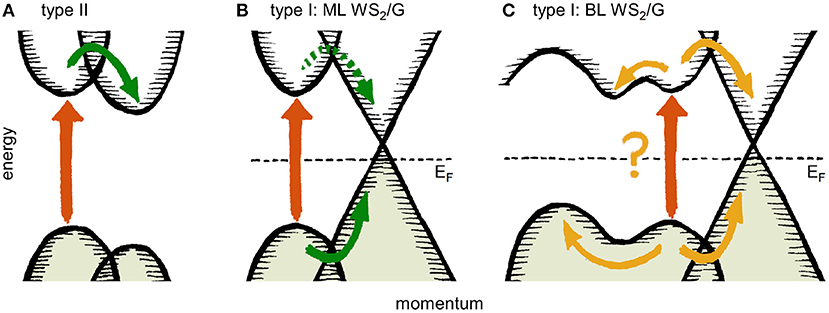
Figure 1. Influence of band alignment on ultrafast charge transfer in different van der Waals heterostructures. (A) Example of a heterostructure with type II band alignment favoring electron transfer. (B) Type I band alignment of a heterostructure made of monolayer WS2 and monolayer graphene. Both electrons and holes are found to transfer to the graphene layer albeit at different rates resulting in ultrafast charge separation. (C) Band alignment of a heterostructure made of bilayer WS2 and monolayer graphene. The influence of the indirect band gap on the microscopic scattering channels mediating ultrafast charge transfer remains unexplored.
One simple way to improve the efficiency of WS2/graphene-based light harvesting devices might be to enhance the thickness and therefore the absorption of the WS2 layer [18–20]. It is not a priori clear, however, if ultrafast charge separation survives when direct-gap monolayer WS2 is replaced by thicker WS2 layers with an indirect band gap (Figure 1C). In this work we address this issue by exciting carriers across the direct gap at the K-point of BL WS2 in an epitaxial BL WS2/graphene heterostructure on SiC(0001) and tracing the relaxation of the photogenerated electron-hole pairs as a function of time, energy, and momentum using time- and angle-resolved photoemission spectroscopy (tr-ARPES). We find that photoexcited holes in BL WS2 are transferred to the graphene layer within 100 fs. The photoexcited electrons are found to remain in the conduction band of BL WS2 for 420 fs resulting in the formation of a charge separated transient state with a lifetime of 770 fs. These timescales are consistent with the microscopic charge transfer model recently proposed for ML WS2/graphene heterostructures [13] indicating that also in the case of BL WS2 on graphene the timescale for charge separation is determined by direct tunneling at the points in the Brillouin zone where WS2 and graphene bands intersect.
2. Methods
2.1. Sample Preparation and Characterization
Commercial N-doped 6H-SiC(0001) wafers from SiCrystal GmbH were etched in hydrogen atmosphere and then graphitized by annealing at 1,300°C in argon atmosphere for 8 min [21]. The resulting carbon buffer layer was decoupled from the substrate by hydrogen intercalation at 800°C yielding a completely sp2-hybridized quasi free-standing hole-doped graphene monolayer [22]. WS2 was grown on top of this graphene layer by low pressure chemical vapor deposition (LPCVD) in a standard hot-wall reactor at a pressure of 1 mbar [23, 24]. Argon served as carrier gas with a flow of 80 sccm. WO3 and S precursors with a mass ratio of 1:100 were kept at 900 and 120°C, respectively. The WO3 powder was placed close to the substrate. After growth, the sample was characterized with secondary electron microscopy (SEM), Raman and photoluminescence (PL) spectroscopy, as well angle-resolved photoemission spectroscopy (ARPES).
The SEM picture in Figure 2A shows dark triangular WS2 islands that cover ~ 80% of the graphene layer. The orientation of the triangles reveals the presence of two rotational domains with an angle of 60° between them. From previous low energy electron diffraction measurements on similar samples [11] we deduce that either the ΓK- or the ΓK′-direction of the WS2 islands are aligned with the ΓK-direction of graphene. Further, the topological contrast reveals that ~ 90% of the islands consist of bilayer WS2. This is consistent with the Raman spectrum shown in Figure 2B where the energy of the A1g peak at 417 cm−1 and the intensity ratio between the central peak at 351 cm−1 (2LA+E2g) and the A1g peak of ~ 6 are indicative of bilayer WS2 [25]. From the PL spectrum in Figure 2C we find a quenched A-exciton resonance at 635 nm (1.95 eV) which confirms the presence of bilayer WS2 [26]. The ARPES spectrum in Figure 2D was taken along the along the ΓK-direction. We find that the band structure of the heterostructure is a superposition of the band structures of the constituting materials that are indicated by the white dashed lines [15, 27]. The Dirac cone of graphene is found to be hole-doped with the Dirac-point 300 meV above the Fermi level, EF. As expected for bilayer WS2 [15] the maximum of the WS2 valence band is found to be located at the Γ-point.
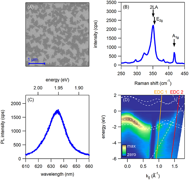
Figure 2. Sample characterization: (A) Secondary electron micrograph revealing triangular WS2 islands with two different rotational domains. The picture was obtained with in lens mode with an accelerating voltage of 5 keV and a beam current of 96 pA. (B) Raman spectrum. Arrows indicate the phonon modes that were used to determine the layer thickness. (C) Photoluminescence (PL) spectrum. Raman and PL measurements were carried out with 1 mW laser excitation at λ = 532 nm at room temperature. (D) ARPES spectrum revealing the occupied part of the band structure of the heterostructure. Orange and red lines indicate the two energy distribution curves (EDCs) that were chosen for the time-resolved measurements in Figure 3. White dashed lines denote theoretical band positions of graphene [27] and bilayer WS2 [15]. A rigid band shift of +0.3 eV was applied to graphene bands to account for the observed p-doping. WS2 CB and VB were rigidly shifted by −0.81 and −1.19 eV, respectively, to match the experimental dispersion. The thin white line marks the position of the Fermi level, EF. At an emission angle of ~ 23° the laser beam was directly reflected into the Time-of-Flight analyzer dazzling the detector and leading to a dark corridor at ~ 0.8 Å−1.
2.2. Tr-ARPES
Tr-ARPES experiments were performed at the Artemis user facility at the Rutherford Appleton Laboratory in Harwell, UK. We used a Ti:Sa amplifier with a central wavelength of 795 nm, a repetition rate of 1 kHz, 30 fs pulse duration, and 12 mJ pulse energy to generate visible pump and extreme ultraviolet (XUV) probe pulses. Two mJ of output energy were focused into an Argon gas jet for high harmonics generation. A single harmonic at ℏωprobe = 31.8 eV was selected with a time-preserving grating monochromator [28] to be used as the probe. Ten mJ of output power were used to seed an optical parametric amplifier. The signal beam with a photon energy of 1 eV was frequency doubled yielding 2 eV pump pulses matching the A-exciton resonance in WS2. The kinetic energy of the photoelectrons emitted from the sample by the XUV probe pulse were measured with a home-built Time-of-Flight analyzer with an angular acceptance of 2° [29]. The static ARPES spectrum in Figure 2D was obtained by rotating the sample. We measured the energy dependence of the photocurrent at two different emission angles (energy distribution curves, EDCs) as a function of pump-probe delay. The energy and temporal resolution of the experiment were 450 meV and 66 fs, respectively.
3. Results
To investigate ultrafast charge transfer in our BL WS2/graphene heterostructure we excited carriers across the direct band gap at the K-point of BL WS2 using 2 eV pump pulses and probed the response of the heterostructure using tr-ARPES. In detail, we investigated the time dependence of two representative energy distributions curves (EDC 1 and EDC 2 in Figure 2D) to obtain the population and band structure dynamics of the WS2 conduction and valence band (CB and VB) and the graphene Dirac cone, respectively. The pump fluence was 6.6 mJ/cm2 for EDC 1 (WS2) and 9.1 mJ/cm2 for EDC 2 (graphene).
Figures 3A,B show EDC 1 and EDC2, respectively, as a function of pump-probe delay. The corresponding pump-induced changes obtained by subtracting the respective EDC at negative pump-probe delay from the transient EDCs are shown in Figures 3C,D. Upon arrival of the pump pulse the WS2 VB is found to shift toward the Fermi level in Figure 3A. This up-shift is responsible for the strong gain (red) and loss (blue) signal around −2 eV in Figure 3C. Figure 3C also reveals a transient gain of photoelectrons in the CB of WS2 around +1 eV following photoexcitation. The graphene π-band in Figure 3B is found to broaden and to shift down which—together with the up-shift of the WS2 VB at lower energy—produces the gain-loss-gain signal in the energy range between +1 and −2 eV in Figure 3D.
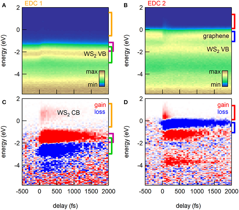
Figure 3. Time- and angle-resolved photoemission spectroscopy (tr-ARPES). (A,B) Time-resolved EDCs measured along the orange (EDC1) and red lines (EDC2), respectively, in Figure 2D as a function of pump-probe delay after photoexcitation at ℏωpump = 2 eV. (C,D) Pump-induced changes of EDC1 and EDC2, respectively, obtained by subtracting the equilibrium EDC taken at negative pump-probe delay from all transient EDCs. Red and blue correspond to gain and loss of photoelectrons with respect to negative pump-probe delay, respectively. Colored brackets indicate the integration ranges for the data presented in Figure 4.
To analyze the transient population dynamics of the individual bands we integrated the EDCs in Figure 3 over the energy range indicated by the colored brackets yielding the pump-probe traces in Figure 4. Panel A shows the transient population of the WS2 VB and CB in green and orange, respectively. The population of the WS2 VB is found to be unaffected by the photoexcitation within the experimental signal-to-noise ratio. The WS2 CB on the other hand exhibits a clear gain of electrons. An exponential fit to the data yields a lifetime of the electrons in the WS2 CB of τ = 420 ± 20 fs. Figure 4B shows the gain above and the loss below the Fermi level in graphene. We find a short-lived gain (τ = 97 ± 3 fs) and a long-lived loss (τ = 840 ± 30 fs). The transient up-shift of the WS2 VB gives rise to a gain of photoelectrons above its equilibrium position that is plotted as a function of pump-probe delay in Figure 4C. An exponential fit to the data yields a lifetime of τ = 770 ± 30 fs.
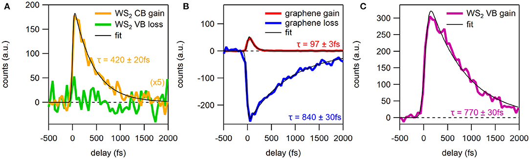
Figure 4. Population dynamics of WS2 and graphene states. (A) Transient occupation of WS2 conduction band (CB, orange) and valence band (VB, green). The curves were obtained by integrating the photocurrent over the energy range marked by the orange and green brackets in Figure 3A for CB and VB, respectively. (B) Transient photocarrier dynamics of graphene. The curves were obtained by integrating the photocurrent over the energy range marked by the red and blue brackets in Figure 3B corresponding to the gain above EF and the loss below EF, respectively. (C) Photocurrent integrated over the energy range marked by the purple bracket in Figure 3C as a function of pump-probe delay. Black lines are exponential fits to data.
In agreement with Aeschlimann et al. [11] and Krause et al. [13], we interpret these timescales as follows: The absence of holes in the WS2 VB together with the short-lived gain in graphene indicates that the photogenerated holes in the WS2 VB are rapidly (within ~ 100 fs) refilled by electrons from the Dirac cone. The photoexcited electrons are found to remain in the WS2 CB for ~ 400 fs, indicating the formation of a charge-separated transient state where the holes reside in the graphene layer and the electrons reside in the WS2 layer. This charge-separated state is expected to decrease the binding energy of the WS2 states and to increase the binding energy of the graphene states [11, 13].
Figures 5A,B illustrate the fitting procedure used to determine the transient peak positions of the WS2 VB and CB and the graphene Dirac cone, respectively. Details are provided in the figure caption. The transient positions of the WS2 CB and VB are shown in Figures 5C,D, respectively. We find that the WS2 VB shifts up by ~ 110 meV with a lifetime of τ = 600 ± 20 fs (Figure 5D). The transient WS2 band gap at k ≈ 1.1 Å−1 obtained by subtracting the transient position of the VB from the transient position of the CB is displayed in Figure 5E. An exponential fit yields a transient band gap reduction of ~230 meV with a lifetime of τ = 140 ± 40 fs. Note that the equilibrium gap size of 2.7 eV at k ≈ 1.1 Å−1 is bigger than the direct band gap at the K-point [13, 30]. In good agreement with Chernikov et al. [31], Liu et al. [32], Ulstrup et al. [33], and Pogna et al. [34], we attribute this band gap renormalization to the presence of photoexcited carriers that screen the Coulomb interaction.
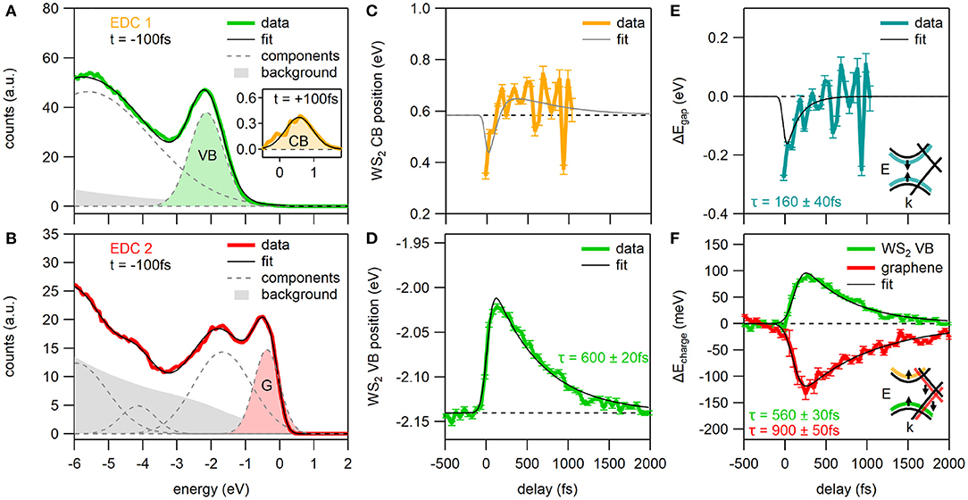
Figure 5. Transient band shifts. (A) EDC1 at negative pump-probe delay together with Gaussian fit. The inset shows the difference EDC1 at the peak of the pump-probe signal used to fit the binding energy of the WS2 CB with a single Gaussian. (B) EDC2 at negative pump-probe delay together with Gaussian fit. Fit components and Shirley background are displayed as dashed gray lines and gray-shaded areas, respectively, in (A,B). The peaks that were used to determine the transients peak positions in (C,D,F) are shaded in the respective colors in (A,B). (C) Transient position of WS2 CB. (D) Transient position of WS2 VB. (E) Transient changes of WS2 band gap calculated by subtracting (D) from (C). (F) Charging shifts of WS2 VB and graphene Dirac cone as a function of pump-probe delay. Black lines are exponential fits to the data.
The transient band gap renormalization results in shifts of the WS2 VB and CB that are symmetric with respect to the center of the WS2 band gap (see inset of Figure 5E). By subtracting |ΔEgap|/2 from the transient position of the WS2 VB we obtain the transient VB shift shown in green in Figure 5F that shows a remaining up-shift of ~ 90 meV with a lifetime of τ = 560 ± 30 fs. At the same time the π-bands of graphene shown in red in Figure 5F shift down by ~ 110 meV with a lifetime of τ = 900 ± 50 fs. As discussed previously, these shifts are a direct consequence of the transient charge-separated state where excess negative charge on the WS2 layer decreases the binding energy of the WS2 states and the corresponding excess positive charge on the graphene layer increases the binding energy of the graphene states. These charging shifts are sketched in the inset of Figure 5F. At this point we are able to attribute the pump-probe signal in Figure 4C to the transient up-shift of the WS2 layer the lifetime of which is linked to the lifetime of the charge-separated state [13]. Also, the dynamics of the WS2 CB shown in Figure 5C can now be explained by the combined effect of band gap renormalization that increases the binding energy of the WS2 CB on the timescale of the photoexcitation and charging that decreases the binding energy of the WS2 CB on the timescale of the hole transfer.
All things considered, our data reveals a detailed picture of the ultrafast charge separation following photoexcitation of the WS2/graphene heterostructure. We find that (1) hole transfer from WS2 to graphene occurs within ~ 100 fs, (2) photoexcited electrons remain inside the WS2 CB for ~ 400 fs, and (3) the charge-separated state decays within ~ 800 fs (This number corresponds to the average of the lifetimes of the graphene loss in Figure 4B, the WS2 VB gain in Figure 4C and the charging shifts in Figure 4F).
4. Discussion
The observed lifetimes for electron and hole transfer are in good agreement with previous tr-ARPES [11, 13] and time-resolved optical techniques [12] on similar WS2/graphene heterostructures. Next we will discuss if the microscopic model for ultrafast charge separation across the interface between monolayer WS2 and monolayer graphene [13] also applies to heterostructures made of bilayer WS2 and monolayer graphene. In this model [13], the timescale for ultrafast charge separation in the heterostructure is determined by direct tunneling of hot carriers from WS2 to graphene at those points in the Brillouin zone where the respective bands intersect. The associated energy barrier is smaller for holes than for electrons which, combined with a larger tunneling matrix element and a larger scattering phase space, results in hole transfer being faster than electron transfer. The lifetime of the charge separated state, on the other hand, is determined by defect-assisted tunneling via in-gap states originating from S vacancies inside the WS2 layer. This decay channel is extremely sensitive to the number of S vacancies in the sample, resulting in lifetimes of the transient charge-separated state between ~ 1 ps in high-quality epitaxial samples [11, 13] and > 1 ns in commercial manually assembled heterostructures [12]. In this model ultrafast charge transfer occurs close to the K-point of WS2 where the WS2 VB maximum and CB minimum are located.
It is not a priori clear whether this model also applies to heterostructures made of bilayer WS2 and monolayer graphene because, in this case, the maximum of the WS2 VB and the minimum of the WS2 CB are located at Γ and Σ (in between Γ and K), respectively. The observed timescales for hole transfer from WS2 to graphene within ~ 100 fs and a lifetime of the electrons inside the WS2 CB at K of ~ 400 fs are perfectly consistent with direct tunneling via band intersections close to the K-point. The lifetime of the charge-separated transient state of ~ 800 fs observed in the present heterostructure is consistent with defect-assisted tunneling via S vacancies in similar high-quality epitaxial samples [11, 13]. Therefore, we conclude that, despite the band structure differences, the microscopic model for ultrafast charge transfer developed for the interface between monolayer WS2 and monolayer graphene [13] also applies for heterostructures made of bilayer WS2 and monolayer graphene (see sketch in Figure 6).
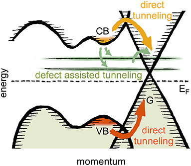
Figure 6. Sketch of microscopic charge transfer model. Thick yellow and red arrows indicate direct tunneling of electrons and holes, respectively, through the crossing points of the respective bands. Green arrows indicate defect-assisted tunneling of electrons via S vacancies inside the WS2 layer.
In summary, we have shown that ultrafast charge separation also occurs at the interface between bilayer WS2 and monolayer graphene. Together with the enhanced absorption in the visible spectral range compared to monolayer WS2 our findings provide important insights that will guide the design of novel optoelectronic applications.
Data Availability Statement
The raw data supporting the conclusions of this article will be made available by the authors upon request.
Author Contributions
IG, CCa, ES, and CCo organized the project. SF, FF, AR, and CCo prepared the sample. RK, MC-C, SA, SF, FF, AR, YZ, PM, RC, CCa, and IG prepared and conducted the tr-ARPES experiments. RK analyzed the data. RK and IG wrote the manuscript. All authors contributed to manuscript revision, read, and approved the submitted version.
Funding
This project has received funding from the European Union's Horizon 2020 research and innovation programme under Grant Agreement No. 654148 Laserlab-Europe, no. 785219 Graphene Core2, and no. 881603 Graphene Core3, from the Deutsche Forschungsgemeinschaft through CRC 925 and CRC 1277 and from UK EPSRC (Grant GR/M50447).
Conflict of Interest
The authors declare that the research was conducted in the absence of any commercial or financial relationships that could be construed as a potential conflict of interest.
References
1. Skoplaki E, Palyvos JA. On the temperature dependence of photovoltaic module electrical performance: a review of efficiency/power correlations. Solar Energy. (2009) 83:614–24. doi: 10.1016/j.solener.2008.10.008
2. King RR, Law DC, Edmondson KM, Fetzer CM, Kinsey GS, Yoon H, et al. Advances in high-efficiency III-V multijunction solar cells. Adv Optoelectron. (2007) 2007:1–8. doi: 10.1155/2007/29523
3. Wang G, Chernikov A, Glazov MM, Heinz TF, Marie X, Amand T, et al. Colloquium: excitons in atomically thin transition metal dichalcogenides. Rev Mod Phys. (2018) 90:021001. doi: 10.1103/RevModPhys.90.021001
4. Bernardi M, Palummo M, Grossman JC. Extraordinary sunlight absorption and one nanometer thick photovoltaics using two-dimensional monolayer materials. Nano Lett. (2013) 13:3664–70. doi: 10.1021/nl401544y
5. Hong X, Kim J, Shi SF, Zhang Y, Jin C, Sun Y, et al. Ultrafast charge transfer in atomically thin MoS2/WS2 heterostructures. Nat Nanotechnol. (2014) 9:682–6. doi: 10.1038/nnano.2014.167
6. Ceballos F, Bellus MZ, Chiu HY, Zhao H. Ultrafast charge separation and indirect exciton formation in a MoS2-MoSe2 van der Waals heterostructure. ACS Nano. (2014) 8:12717–24. doi: 10.1021/nn505736z
7. Zhu X, Monahan NR, Gong Z, Zhu H, Williams KW, Nelson CA. Charge transfer excitons at van der Waals interfaces. J Am Chem Soc. (2015) 137:8313–20. doi: 10.1021/jacs.5b09894
8. Chen H, Wen X, Zhang J, Wu T, Gong Y, Zhang X, et al. Ultrafast formation of interlayer hot excitons in atomically thin MoS2/WS2 heterostructures. Nat Commun. (2016) 7:12512. doi: 10.1038/ncomms12512
9. Rivera P, Schaibley JR, Jones AM, Ross JS, Wu S, Aivazian G, et al. Observation of long-lived interlayer excitons in monolayer MoSe2–WSe2 heterostructures. Nat Commun. (2015) 6:6242. doi: 10.1038/ncomms7242
10. Merkl P, Mooshammer F, Steinleitner P, Girnghuber A, Lin KQ, Nagler P, et al. Ultrafast transition between exciton phases in van der Waals heterostructures. Nat Mater. (2019) 18:691–6. doi: 10.1038/s41563-019-0337-0
11. Aeschlimann S, Rossi A, Chávez-Cervantes M, Krause R, Arnoldi B, Stadtmüller B, et al. Direct evidence for efficient ultrafast charge separation in epitaxial WS2/graphene heterostructures. Sci Adv. (2020) 6:eaay0761. doi: 10.1126/sciadv.aay0761
12. Fu S, Fossé Id, Jia X, Xu J, Yu X, Zhang H, et al. Long-lived charge separation following pump-energy dependent ultrafast charge transfer in graphene/WS2 heterostructures. arXiv. (2020) 200708932. doi: 10.1126/sciadv.abd9061
13. Krause R, Aeschlimann S, Chavez-Cervantes M, Perea-Causin R, Brem S, Malic E, et al. Microscopic understanding of ultrafast charge transfer in van-der-Waals heterostructures. arXiv. (2020) 201209268.
14. Zhu ZY, Cheng YC, Schwingenschlögl U. Giant spin-orbit-induced spin splitting in two-dimensional transition-metal dichalcogenide semiconductors. Phys Rev B. (2011) 84:153402. doi: 10.1103/PhysRevB.84.153402
15. Zeng H, Liu GB, Dai J, Yan Y, Zhu B, He R, et al. Optical signature of symmetry variations and spin-valley coupling in atomically thin tungsten dichalcogenides. Sci Rep. (2013) 3:1608. doi: 10.1038/srep01608
16. Novoselov KS, Geim AK, Morozov SV, Jiang D, Katsnelson MI, Grigorieva IV, et al. Two-dimensional gas of massless Dirac fermions in graphene. Nature. (2005) 438:197–200. doi: 10.1038/nature04233
17. Avsar A, Ochoa H, Guinea F, Özyilmaz B, van Wees BJ, Vera-Marun IJ. Colloquium: spintronics in graphene and other two-dimensional materials. Rev Mod Phys. (2020) 92:021003. doi: 10.1103/RevModPhys.92.021003
18. Zhao W, Ghorannevis Z, Chu L, Toh M, Kloc C, Tan PH, et al. Evolution of electronic structure in atomically thin sheets of WS2 and WSe2. ACS Nano. (2012) 7:791–7. doi: 10.1021/nn305275h
19. Zhu B, Chen X, Cui X. Exciton binding energy of monolayer WS2. Sci Rep. (2015) 5:9218. doi: 10.1038/srep09218
20. Raja A, Selig M, Berghäuser G, Yu J, Hill HM, Rigosi AF, et al. Enhancement of exciton–phonon scattering from monolayer to bilayer WS2. Nano Lett. (2018) 18:6135–43. doi: 10.1021/acs.nanolett.8b01793
21. Emtsev KV, Bostwick A, Horn K, Jobst J, Kellogg GL, Ley L, et al. Towards wafer-size graphene layers by atmospheric pressure graphitization of silicon carbide. Nat Mater. (2009) 8:203–7. doi: 10.1038/nmat2382
22. Riedl C, Coletti C, Iwasaki T, Zakharov AA, Starke U. Quasi-free-standing epitaxial graphene on SiC obtained by hydrogen intercalation. Phys Rev Lett. (2009) 103:246804. doi: 10.1103/PhysRevLett.103.246804
23. Rossi A, Büch H, Rienzo CD, Miseikis V, Convertino D, Al-Temimy A, et al. Scalable synthesis of WS2 on graphene and h-BN: an all-2D platform for light-matter transduction. 2D Mater. (2016) 3:031013. doi: 10.1088/2053-1583/3/3/031013
24. Forti S, Rossi A, Büch H, Cavallucci T, Bisio F, Sala A, et al. Electronic properties of single-layer tungsten disulfide on epitaxial graphene on silicon carbide. Nanoscale. (2017) 9:16412–9. doi: 10.1039/C7NR05495E
25. Berkdemir A, Gutiérrez HR, Botello-Méndez AR, Perea-López N, Elías AL, Chia CI, et al. Identification of individual and few layers of WS2 using Raman Spectroscopy. Sci Rep. (2013) 3:1755. doi: 10.1038/srep01755
26. Li Y, Li X, Yu T, Yang G, Chen H, Zhang C, et al. Accurate identification of layer number for few-layer WS2 and WSe2 via spectroscopic study. Nanotechnology. (2018) 29:124001. doi: 10.1088/1361-6528/aaa923
28. Frassetto F, Bryan W, Cacho C, Turcu E, Springate E, Poletto L. Time-preserving grating monochromator for extreme-ultraviolet ultrashort pulses. J Phys Conf Ser. (2013) 425:122006. doi: 10.1088/1742-6596/425/12/122006
29. Cacho CM, Vlaic S, Malvestuto M, Ressel B, Seddon EA, Parmigiani F. Absolute spin calibration of an electron spin polarimeter by spin-resolved photoemission from the Au(111) surface states. Rev Sci Instrum. (2009) 80:043904. doi: 10.1063/1.3115213
30. Chernikov A, Berkelbach TC, Hill HM, Rigosi A, Li Y, Aslan OB, et al. Exciton binding energy and nonhydrogenic rydberg series in monolayer WS2. Phys Rev Lett. (2014) 113:076802. doi: 10.1103/PhysRevLett.113.076802
31. Chernikov A, Ruppert C, Hill HM, Rigosi AF, Heinz TF. Population inversion and giant bandgap renormalization in atomically thin WS2 layers. Nat Photonics. (2015) 9:466–70. doi: 10.1038/nphoton.2015.104
32. Liu F, Ziffer ME, Hansen KR, Wang J, Zhu X. Direct determination of band-gap renormalization in the photoexcited monolayer MoS2. Phys Rev Lett. (2019) 122:246803. doi: 10.1103/PhysRevLett.122.246803
33. Ulstrup S, Cabo AG, Miwa JA, Riley JM, Grønborg SS, Johannsen JC, et al. Ultrafast band structure control of a two-dimensional heterostructure. ACS Nano. (2016) 10:6315–22. doi: 10.1021/acsnano.6b02622
Keywords: TMD, graphene, van der Waals heterostructures, tr-ARPES, ultrafast charge transfer, photovoltaics
Citation: Krause R, Chávez-Cervantes M, Aeschlimann S, Forti S, Fabbri F, Rossi A, Coletti C, Cacho C, Zhang Y, Majchrzak PE, Chapman RT, Springate E and Gierz I (2021) Ultrafast Charge Separation in Bilayer WS2/Graphene Heterostructure Revealed by Time- and Angle-Resolved Photoemission Spectroscopy. Front. Phys. 9:668149. doi: 10.3389/fphy.2021.668149
Received: 15 February 2021; Accepted: 23 March 2021;
Published: 29 April 2021.
Edited by:
Gang Zhang, Institute of High Performance Computing, Agency for Science, Technology and Research (A*STAR), SingaporeReviewed by:
Yuriy Dedkov, Shanghai University, ChinaDavid R. Heskett, University of Rhode Island, United States
Copyright © 2021 Krause, Chávez-Cervantes, Aeschlimann, Forti, Fabbri, Rossi, Coletti, Cacho, Zhang, Majchrzak, Chapman, Springate and Gierz. This is an open-access article distributed under the terms of the Creative Commons Attribution License (CC BY). The use, distribution or reproduction in other forums is permitted, provided the original author(s) and the copyright owner(s) are credited and that the original publication in this journal is cited, in accordance with accepted academic practice. No use, distribution or reproduction is permitted which does not comply with these terms.
*Correspondence: Razvan Krause, razvan.krause@ur.de; Isabella Gierz, isabella.gierz@ur.de