 Anna Vignati1,2*
 Simona Giordanengo2
 Federico Fausti2,3
 Oscar A. Martì Villarreal1,2
 Felix Mas Milian1,4
 Giovanni Mazza2
 Zahra Shakarami1,2
 Roberto Cirio1,2Vincenzo Monaco1,2
 Roberto Sacchi1,2
- 1Physics Department, Università degli Studi di Torino, Turin, Italy
- 2INFN—National Institute for Nuclear Physics, Turin Division, Turin, Italy
- 3DE.TEC.TOR. Devices & Technologies Torino S.r.l., Turin, Italy
- 4Department of Exact and Technological Sciences (DCET), Universidade Estadual de Santa Cruz, Ilhéus, Brazil
The emergent FLASH RadioTherapy (RT) uses ultrahigh dose-rate irradiation (up to 107 Gy/s instantaneous dose-rate in each μs pulse) to deliver a single high dose of irradiation in a very short time (<200 ms). Pre-clinical studies at ultrahigh dose-rates recently showed an increased ratio between tumoricidal effect and normal tissue toxicity (therapeutic index), compared to conventional RT at standard Gy/min dose-rates. If confirmed by biological in vivo validations, this could represent a breakthrough in cancer treatment. However, the reliability and the accuracy of experimental studies are nowadays limited by the lack of detectors able to measure online the beam fluence at FLASH dose-rates. The behavior of standard beam monitors (gas-filled ionization chambers) is compromised by the volume recombination caused by the amount of charges created per unit volume and unit time, due to the large dose-rate. Moreover, due to the lack of proper monitoring devices and to the uncertainties of its future applications, very few facilities are able to deliver at present FLASH irradiations. In this contribution, we report about the physical and technological challenges of monitoring high and ultra-high dose-rates with electrons and photon beams, starting from the pre-clinical and clinical constraints for new devices. Based on the extensive experience in silicon detectors for monitoring applications in RT with external beams, the work then investigates silicon sensors as a possible option to tackle such extreme requirements and a rugged thin and large (e.g., 10 × 10 cm2) flat detector (silicon-based sensor + readout electronics) is therefore outlined. This study aims at presenting the FLASH-RT dosimetry problem and analyzing the possibilities for a silicon sensor to be employed as sensing device for several FLASH scenarios, including some ideas on the readout part. However, more detailed simulations and studies are demanded to delineate more precisely the technical choices to be undertaken in order to tackle the clinical accuracy required on the beam fluence, typically a few %, during photon and electron high and ultra-high irradiations, the required minimal perturbation of the beam and the high level of radiation resistance.
Introduction
A typical Radiotherapy (RT) treatment delivers a total dose of 20–80 Gy to the target in tens of fractions (generally, 2 Gy per fraction) to fulfill the dose constraints due to normal tissue complications. The irradiation duration depends on the accelerators: present kV and MV sources provide dose-rates ranging from 0.5 to 10 Gy/min.
In parallel, the emergent and highly promising FLASH RT is proposing a completely different dose fractionation, which consists in the delivery of a single irradiation at ultrahigh instantaneous dose-rates (up to 107 Gy/s in each μs pulse) in a very short time (<200 ms) [1, 2].
This technique has recently drawn great attention because of the reduced toxicity at the normal tissue level observed in pre-clinical studies on cells and animals, compared to conventional RT at standard dose-rates [3]. Moreover, at the time of writing, the first patient, affected by a highly resistant skin lymphoma, was treated with FLASH modality, with an impressive early result [4]. If confirmed by ongoing research and biological in vivo validations, this could represent a breakthrough in cancer treatment.
However, biological validations in vivo are mandatory to bring the needed global consensus on FLASH, but the reliability and the accuracy of experimental studies are nowadays limited by the lack of traceable active detectors. Standard beam monitors (gas-filled ionization chambers), in fact, cannot be used for ultrahigh dose-rates, because of the high rate of charge recombination. Additionally, ionization chambers need several tens of μs (30–300 μs for 0.5–5 mm air gap) to collect the ions [5] and are too slow to control a FLASH beam, which delivers tens of Gy in a few μs.
Due to the lack of proper monitoring devices, and the uncertainties of its future applications, very few facilities are able to deliver, at present, ultrahigh dose-rate irradiation, and these mostly provide electron and proton beams [3].
On the other side, a number of advanced devices, mainly based on silicon diodes, have been developed to reliably measure the complex delivered dose-map achievable with modern RT techniques [6]. Starting from the results obtained with these devices, this work aims at studying and defining the characteristics of a rugged, thin and large silicon detector able to monitor the dose during photon and electron FLASH irradiations.
In the following, we report the physical characteristics of FLASH beams, the principles of the online dose delivery, and the requirements for a new beam monitor. The work then describes the results obtained by simulating the behavior of a new silicon detector on ultrahigh dose-rates irradiations and the related open issues.
Materials and Methods
In the same way as conventional RT, the FLASH treatment outcome will strongly rely on the dose delivery accuracy, at both the particle accelerator level and the beam shaping and monitoring system, including the detectors for the online measurements of the main beam parameters.
In this section, we present the physical characteristics of FLASH beams, which impose new challenges for the next generation of detectors mandatory to guarantee the patient safety and treatment accuracy with FLASH irradiations. The main features of the existing beam monitors are rapidly reviewed before describing the characteristics of the new silicon detector, assumed as a viable option to tackle the challenging of monitoring FLASH beams.
FLASH Beam Characteristics
Dose Rates
X-rays and electrons used in conventional RT are produced by linear accelerators (LINAC) in which radiofrequency (RF) waves periodically accelerate the electrons providing pulsed radiation output.
The pulse duration is controlled by the pulse modulator and ranges from 2 to 6 μs, while the pulse repetition frequency (PRF) is usually adjustable in discrete values, typically from 50 to 1,000 Hz, by the PRF generator [7, 8]. This means that the existing accelerators show duty cycles from 0.01 to 0.6%.
The beam delivery time structure is crucial for FLASH treatments because the requirement of a specific mean dose-rate, typically >40 Gy/s, entails a much higher pulsed dose-rate during the duty cycle of the accelerator. For example, considering a LINAC with pulse duration of 6 μs and PRF of 1,000 Hz, or 1 ms period (see the blue example in Figure 1), a FLASH mean dose-rate of 100 Gy/s can be delivered in 6 μs pulses with instantaneous dose-rates of 16 kG/s. At the other extreme, with a pulse duration of 2 μs and PRF of 50 Hz, the same average dose-rate requires an instantaneous dose-rate 60 times larger. The FLASH instantaneous dose-rates reported in literature range from 103 Gy/s up to 106 Gy/s for photons and even higher (107 Gy/s) for electrons [1, 9].
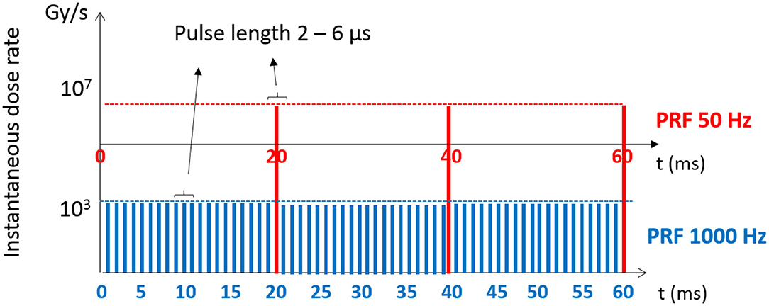
Figure 1. Flash instantaneous dose-rate for an average dose-rate of 100 Gy/s delivered by a LINAC working at two different PRF: 50 and 1,000 Hz.
Beam Monitors in Conventional Radiotherapy
The beam monitor consists of a set of transmission ionization chambers, covering the whole cross sectional area of the radiation beam, which are designed to monitor the delivered dose and dose-rate, as well as additional operating parameters such as beam flatness and symmetry [10]. During irradiation, the charge collected in each chamber is quantified in terms of Monitor Units (MU), calibrated to correspond to 1 cGy dose in standard reference conditions. Once the pre-set number of MUs has been reached in the primary ionization chamber, the irradiation is terminated. At present, a secondary chamber is required for redundancy: if the primary chamber fails, underestimating the dose, the second one is used to terminate the treatment. To avoid sensitivity changes resulting from fluctuations in temperature and pressure, these chambers may be sealed or vented and are properly calibrated according to the measured gas temperature and pressure. They are thin and use low atomic number materials for their entry and exit windows, to be as transparent as possible to the beam. In addition to being part of all the beam delivery systems in all clinical RT facilities, gas-filled ionization chambers are also used for commissioning of RT LINAC [11] and for Quality Assurance (QA). Because of their limited complexity and simple mechanical construction, they offer several advantages such as robustness, ease of operation, and show no indication of performance degradation due to aging effects, even after several years of irradiation.
FLASH irradiations cause a radical change in the beam characteristics, in the delivery time structure and, above all, in the average and instantaneous dose-rate (see section FLASH Beam Characteristics), which points-out the limits of ionization chambers. Although correction factors have been shown to be effective up to 2 kGy/s [12], nevertheless ionization chambers cannot be used for ultrahigh dose-rates, because of the high rate of recombination. The latter depends on the amount of charges created per unit volume and unit time, i.e. on the dose-rate, which is the quantity to be measured. Although specific models have been recently developed to characterize the saturation and compute the absolute dose, this saturation effect may vary depending on the beam characteristics and irradiation setup, which makes the establishment of the correction factors inaccurate and time-consuming [13]. Additionally, ionization chambers need several tens of μs (30–300 μs for 0.5–5 mm air gap) to collect the charges and are too slow to monitor a FLASH beam, which delivers tens of Gy in a few μs.
This scenario clearly draws the need of new monitoring devices, essential to perform thorough pre-clinical studies on the biological mechanisms underpinning the effectiveness of FLASH therapy, and we here explore silicon detectors as a viable option, among alternative technologies that can be considered.
Silicon Detector
Silicon devices have been early proposed for dosimetry in RT [14], because of the well-developed manufacturing technology, their high sensitivity (tens of thousand times larger than ionization chambers with same active volume) and excellent spatial resolution, and find nowadays application ranging from QA procedures to in vivo dosimetry. Indeed, in the last decades, modern RT techniques started challenging the role of ionization chambers. Tomotherapy, Cyberknife, Intensity Modulated Radiotherapy (IMRT), and Volumetric Modulated Arc Therapy (VMAT) produce radiation closely shaped on the target tumor volume. This is performed by complex radiation fields, characterized by high dose gradients and strong variations in space and time of both dose-rate and beam energy spectrum. Ionization chambers are not recommended for measurements in high dose gradients, as they greatly suffer from both low sensitivity and low spatial resolution. Thus, in recent years, a number of advanced devices, mainly based on silicon diodes, have been developed to reliably measure the delivered dose-map, meeting the requirements of conformal radiation monitoring for clinical RT [6].
On the contrary, thin planar silicon devices have never been used so far as on-line monitoring systems on therapeutic beam lines, as gas-filled ionization chambers currently represent the state-of-the-art for beam monitoring during RT treatments. For beam monitoring of both electrons and photons at ultrahigh dose-rate irradiations the choice of the proper silicon technology (hybrid or monolithic), the design and development of the proper geometry for the silicon sensor in terms of surface and thickness of the single element (pixel/strip) and segmentation (number of elements in the detector) are still to be defined.
The major parameters to be considered in the design regard the instantaneous dose-rates that range from 103 Gy/s up to 107 Gy/s, the final detector size and the distance at which the detector will be positioned with respect to the source. The needed sensitive area is at minimum 10 × 10 cm2 to allow the replacement of the monitor chambers currently used by LINACs, but should be made larger if a larger distance is needed. Indeed, the detector position into the nozzle leads to very different fluence rates, increasing by two orders of magnitude, when the detector is moved from one meter distance from the source to the closest point to the source itself. This implies very different requirements from both silicon detector and electronics point of views, to maintain the same charge collection efficiency, and therefore the same accuracy in the dose-rate measurements.
In this work, the typical FLASH dose-rates were used to simulate the fluence rate of electrons and photons on the silicon sensor surface and the rate of charge generated in a detector element as a function of its sensitive area, sensor thickness and of the particle energy. A substantial number of unknown factors, as for example the onset of plasma conditions within the silicon, which could lead to short-circuit, or the dose-rate dependence represent a big issue. Therefore, the study of the recombination effect, saturation, and sensor linearity with dose-rate, along with possible strategies to correct for those effects and to identify the limits of such corrections, is a fundamental step, which still need to be considered. To tackle the new challenges, detailed simulations and modeling of the detector behavior in such a large flux environment must be done and benchmarked against, for example, passive dosimetry.
Front-End Readout
Given the ultrahigh dose-rates expected in FLASH irradiations, a large segmentation of the sensor is required to limit the current to readout from each channel. Thin pixelated sensors, covering the cross sectional area of the beam, readout by a fully custom front-end ASIC bump bonded to the sensor offer the possibility of combining flux measurement and spatial information in a unique compact detector. The front-end ASIC should be designed to readout the charge in the sensor channel dealing with the high peak pulsed current of FLASH beams, avoiding the amplifier saturation and without dead-time during the beam pulses. Two different approaches are described in the following and their main features are summarized in Table 1.
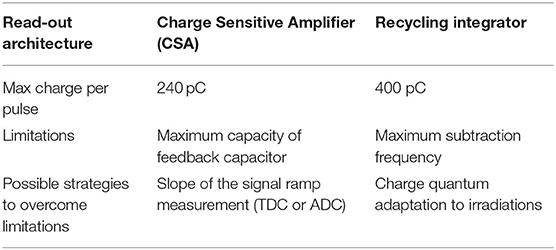
Table 1. Summary of the main characteristics of two possible read-out architectures.
The natural choice for the front-end is the use of a Charge Sensitive Amplifier (CSA), which integrates the input charge on a feedback capacitor Cf, followed by a shaper and an Analog to Digital Converter (ADC) that digitizes the voltage amplitude at the end of each beam pulse. Assuming a modern Complementary Metal-Oxide Semiconductor (CMOS) technology, the capacity density cannot exceed ~100 fF/μm2 leading to a maximum Cf ranging between 10 and 100 pF, depending on the area available over the pixel surface. Using the typical bias voltage of 1.2 V, a maximum charge between 12 and 120 pC (corresponding to a maximum current of 6 and 60 μA for a pulse of 2 μs duration) could be measured in each pulse before saturation of the amplifier. These limits could be increased at most by a factor 2 by using a larger bias voltage for the analog part of the channel (e.g., 2.5 V), while biasing the digital part with a lower voltage.
Different strategies can be implemented to overcome these limits, at the price of increasing the complexity of the front-end design.
Figure 2 shows the block diagram of a modified version of the circuit described above where the slope of the initial ramp of the signal is also measured. In case of saturation of the CSA, the total charge can be recovered from the measured slope using a calibration curve determined experimentally. The slope can be determined by measuring the time taken by the signal to increase from a lower voltage Vth1 to a higher voltage Vth2, using a Time to Digital Converter (TDC) where the start and stop signals are provided by the lower (Vth1) and upper (Vth2) thresholds of a double threshold discriminator, as shown in the lower branch of Figure 2. Alternatively, an ADC can be used to measure the output voltage after a fixed time delay from the start signal provided by a single threshold discriminator. The overall electronics readout uncertainty should be kept at the level of per mill.
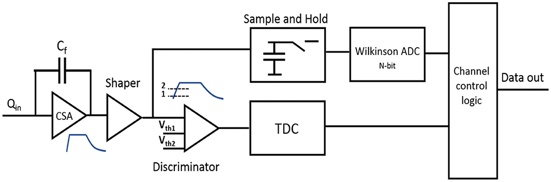
Figure 2. Block diagram of a circuit where an ADC is used to digitize the voltage amplitude at the output of the Charge Sensitive Amplifier (CSA) feedback capacitance, after the entire pulse duration time. The initial slope of the signal is also measured using a TDC and a double threshold discriminator.
A different method, based on a CSA and an active feedback, can be used to limit the amplifier saturation while keeping a dead-time-free front-end readout. This method, based on the recycling integrator architecture, has been applied successfully in several versions of TERA ASICs developed by our group in the last years for particle therapy applications [15]. Referring to Figure 3, when the output of the CSA crosses the discriminator threshold (Vth− for negative and Vth+ for positive input currents), a pulse, generated by the Pulse Generator block, is sent to the Csub capacitor. Two opposite charges, given by the product Csub·(Vpulse+ − Vpulse−) are generated across the capacitor which, with proper synchronization of the two switches shown in the figure, can be used to subtract a constant negative or positive charge quantum, depending on the polarity of the input current, from the charge integrated by the amplifier. With a steady input current, this feedback mechanism prevents data loss caused by the front-end saturation without introducing any deadtime. However, the subtraction mechanism is driven by an external clock and can operate up to a maximum input current, where the maximum subtraction frequency is reached. The number of subtracted charge quanta, stored in a counter, provide a digitized measurement of the input charge. A fast access to the counter may also provide the possibility of monitoring the charge during the pulse, if desired.

Figure 3. Example of recycling integrator functional blocks diagram.
Assuming a maximum subtraction frequency of 100 MHz, a charge quantum of 1 pC, and in the worst scenario of pulses of 2 μs duration, a maximum of 200 pC of charge can be subtracted. This extends by the same amount the charge that can integrated before saturation, as calculated above. With the appropriate choice of the feedback capacitor, charges up to 400 pC per pulse could be measured (i.e., up to 200 μA of current during the pulse).
The choice of the charge quantum determines the charge sensitivity of the front-end and hence the sensitivity to the delivered dose. An average number of subtractions per pulse larger than 100 is needed to achieve a 1% sensitivity in each pulse. Considering the worst scenario of a PRF of 50 Hz this would correspond to a sensitivity of 0.02% for the total treatment. Smaller values of the charge quantum would bring the system closer to saturation whereas larger values would degrade the sensitivity to the dose measurement of each single pulse. The readout should allow for varying the charge quantum in a broad range to adapt to all possible irradiation conditions. This could be achieved both by implementing few parallel capacitors that can be independently added via digital configuration lines to obtain the total capacitance Csub and by varying the Vpulse voltages.
The accuracy of the subtraction mechanism is determined by the accuracy of the voltage difference (Vpulse+ − Vpulse−) and of the capacity Csub; although the former can be made very accurate by using external voltage sources, accuracies of ~10% with channel-by-channel variations up to few % are to be expected for the capacity [16]. An accurate calibration of the charge quantum for each channel using an external current source is therefore mandatory to compensate for this effect.
Results
Rate of Charge Production From Photons and Electrons in Silicon
The rate of charge Q generated in a silicon sensor element at the FLASH ultrahigh dose-rate strongly depends on its active area, on the sensor thickness, on the particle energy and on the dose-rate. It can be derived by the following equation:
where ϕ = N/S · Δt is the rate of electrons/photons hitting the sensor per unit surface (fluence rate), S is the active area of the pixel, is the average energy released per particle, W = 3.6 eV is the average energy required to create an electron-hole pair in silicon and e = 1.6 × 10⁻¹⁹ C.
To estimate the average energy released per particle , Monte Carlo simulations using the Geant4 code with the standard electromagnetic interaction physics package, option three1, were performed. Three cases were considered: a monoenergetic photon beam of 1 MeV energy, a photon beam with the energy spectrum of a 6 MV LINAC and a beam of 6 MeV electrons, representative of the electron beam energies used to treat skin and superficial disease [7, 17]. The detector pixel was modeled as silicon box of 1 mm2 surface in the xy plane, and 100 μm in z, which is a typical silicon wafer thickness, and 109 beam particles were distributed uniformly in the xy plane and directed along z, perpendicularly to the sensor surface, as shown in Figure 4a. The silicon pixel volume was divided into 106 voxels of 10 × 10 × 1 μm3 to record the tridimensional distribution of the energy released by impinging photons, electrons and secondary particles, and the resulting energy was normalized by the total number of particles used in the simulation.
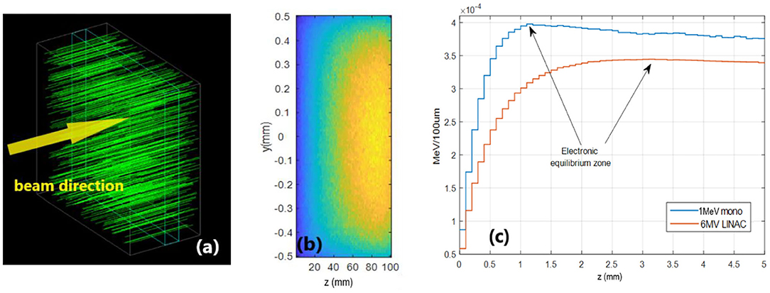
Figure 4. (a) View of the geometry used for the Monte Carlo simulation. (b) Projection in the yz plane of the energy deposited by the 1 MeV photon beam in the sensor. (c) Average deposited energy per photon in 100 μm slices as a function of the depth z in the silicon. Results are shown both for monoenergetic 1 MeV photons and for a photon beam with the energy spectrum of a 6 MV LINAC. The arrows point to the depth where the electronic equilibrium is reached.
Figure 4b shows a projection in the yz plane of the energy deposited by the 1 MeV energy photon beam. The distribution is non-uniform because, given the small thickness of the silicon plane, electrons set in motion by Compton scattered photons lead to an increase of energy deposited with depth, the well-known build-up effect. The build-up occurs within a few millimeters from the surface until electronic equilibrium is reached, as shown in Figure 4c where the simulation was repeated using a thicker silicon absorber to show the effect. It can be observed that the energy deposited in the first 100 μm amounts to <20% of the energy deposited when electronic equilibrium is reached.
Figure 5a shows the average energy deposited in the sensor per photon in 1 μm slices along z, showing the steady increase due to the build-up up to 90 μm, followed by a small decrease due to the lack of the contribution of backscattered particles close to the detector backplane. The corresponding cumulative distribution shown in Figure 5b represents the average energy released per particle () as a function of the detector thickness crossed by the beam. For a 100 μm thick sensor, it amounts to for a monoenergetic 1 MeV beam and for the 6 MV LINAC beam. However, using the smaller thickness of 20 μm, this quantity can be reduced by more than a factor 10 (4.6eV/phot and 3.5eV/phot, respectively).
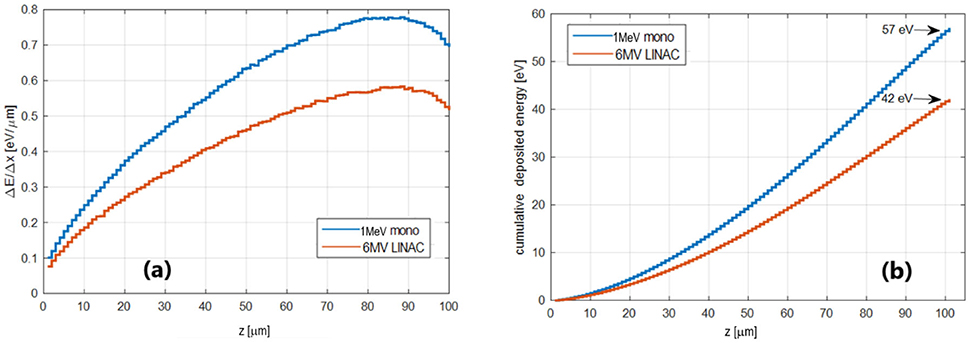
Figure 5. (a) Average energy deposited per photon in 1 μm slices along z. (b) Cumulative deposited energy per photon as a function of the traversed thickness. In each subfigure, the two curves refer to a monoenergetic 1 MeV beam and to a 6 MV LINAC beam.
The study was repeated for a 6 MeV electron beam, showing a more uniform energy deposition about three orders of magnitude larger than for photons, ~0.4keV/μm per particle, leading to for a 100 μm thick sensor.
Although considering the dependence of the energy loss distribution from the thickness of the silicon sensor [18], we decided to assume a constant energy deposition per unit length of 0.4keV/μm. Thus, we accepted an error of a factor 2 in the worst case, acknowledging that the present work aims at providing an approximated evaluation of the orders of magnitude involved in the FLASH irradiations scenarios.
In order to relate the fluence rate of photons passing through the sensor (ϕ in Equation 1) to the dose-rate ΔD/Δt, a rough estimation can be obtained from the photon intensity attenuation law
where Io is the incident intensity, I the transmitted intensity, μ the linear attenuation coefficient and x the absorber thickness. The intensity variation ΔI = I0 − I thus represents the deposited energy ΔE per unit of time and surface in thickness x. For a small thickness one obtains
where ϕ = N/S · Δt is the fluence rate of photons of energy Eo. The dose-rate, i.e., the deposited energy ΔE per unit of mass and time in thickness x, can be expressed using Equation 3 as
leading to the following relation between particle fluence rate and dose-rate:
As an example, for a photon beam with Eo = 1 MeV, delivering a dose-rate of 1 Gy/s, and using , the fluence rate would be .
However, in the medical practice, the dose is defined using a standard procedure because the conversion from dose to particle beam fluence depends on the field parameters and on the procedure used to measure the dose. Indeed, in the standard protocols, the dose is measured at the depth of the dose maximum in a water phantom (with a surface at the isocenter of the machine, i.e., usually at 100 cm from the source) along the axis of a square 10 × 10 cm2 uniform irradiation field [7, 8].
A Monte Carlo simulation using the Geant4 code was performed to estimate the reference dose. Parallel beams of photons with 1 MeV energy, photons with 6 MV LINAC energy spectrum and electrons of 6 MeV were used as sources to deliver a 10 × 10 cm2 uniform field of dose in a 40 × 40 × 40 cm3 water phantom. The phantom was divided into 64,000 voxels of 1 cm3 volume where the average dose was determined as the energy released in the voxel divided by the voxel mass.
In Figure 6, the upper plots show the dose distribution map in the central yz plane obtained with the three simulated beams, whereas the lower plots show the dose as a function of the phantom depth along the central axis of the irradiated field. Following the standard procedure, the dose Dmax is the dose measured at the maximum along the central axis of the irradiation field (lower plot in Figure 6). For each of the three simulations, the number Nsim of particles used is also reported. From these results, the particle fluence rate ϕ for a given dose-rate ΔD/Δt can be expressed as follows
where A = 10 × 10 cm2 represents the field size.
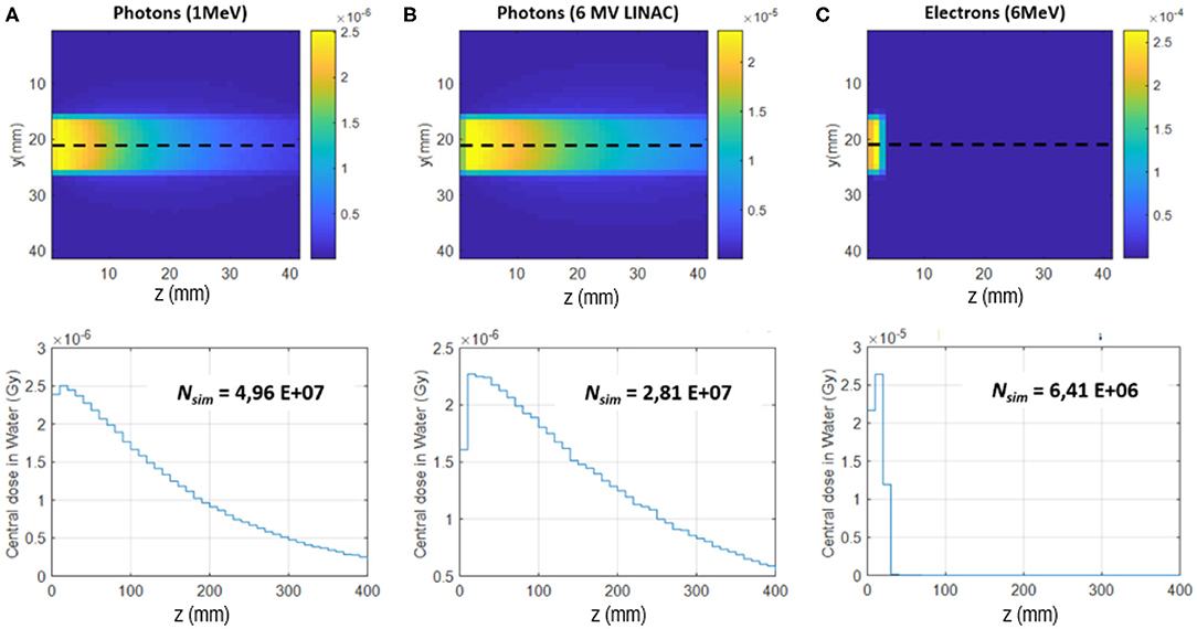
Figure 6. Upper plots: simulated dose distribution maps expressed in Gy, averaged in 1 cm3 voxels, in the central yz plane. Lower plots: dose distributions along the central axis (i.e., along the dotted lines of the upper plots). The results correspond to a 10 × 10 cm2 uniform field in a 40 × 40 × 40 cm3 water phantom irradiated with (A) 1 MeV monoenergetic photons, (B) photons from 6 MV LINAC, and (C) 6 MeV electrons. The number of particles Nsim used in the simulation is reported.
Considering for example a dose-rate of 1 Gy/s, Equation 6 yields the following fluence rates
for the 1 MeV photon beam, for photon beam of a 6 MV LINAC, and for the 6 MeV electron beam, respectively. The fluence rates for photons are found to be in agreement with the rough calculation based on Equation 5.
From these values, weighted with the actual dose-rate, and using Equation 1, the rate of charge production in the silicon can be derived for different beams, dose-rates, sensor area, and thickness.
Table 2 reports the expected rate of charge production in the silicon bulk of the sensor element, together with the total charge produced in a pulse of 5 μs duration, for different scenarios: large (1 mm2) and small (50 × 50 μm2) pixel sizes, normal (100 μm) and very thin (20 μm) sensors, lower and upper limit of the FLASH instantaneous dose-rates as reported in the literature.

Table 2. Rate of charge production and total charge produced in a pulse of 5 μs (in parenthesis) in the detector element for different beams, dose-rates, pixel area, and sensor thickness.
Discussion
FLASH irradiations require the development of new systems for monitoring the beam fluence at the ultrahigh dose-rates. The detectors will have to be compliant with the requirements of the pre-clinics and clinics environments to develop a full system, 100% reliable, able to work within the existing accelerator facilities.
The potentials and limits of silicon detectors, well-known in conventional RT for relative dose verification, are studied in these extremely challenging conditions. According to the preliminary studies reported in this work, the design of a silicon sensor and its readout-electronics requires a remarkable technological effort to allow reading out the charge produced in FLASH beam pulses.
As shown in Table 2, the active thickness of the sensors will need to be reduced down to a few tens of microns. Indeed, it is found that, for photon beams, a reduction of the thickness from 100 to 20 μm lowers the energy released by over a factor 10. In order to limit the charge build-up effect into the sensor, the active area should be exposed to the beam with the minimum of dead material in front of it. Processing technologies which combine back-side reading with thinning procedures via wet etching [19] can be exploited to achieve this goal. Thin sensors have the additional benefit, given the small charge collection time, of reducing the charge recombination probability in the silicon, leading to a better performance, especially at large fluences [20]. Reducing the pixel area allows cutting down the charge produced in each sensor element, but increases the number of readout channels and reduces the area available for the circuit front-end implementation. On the other hand, the readout of an increasing number of pixels would require the implementation of data reduction strategies to avoid transmitting unnecessary information.
In order to find the best compromise and optimize the detector design, each of the above-mentioned aspects must be properly considered, and other effects need to be taken into account with accurate simulations, such as the contribution to the energy deposited in the sensor of backscattered particles.
The data reported in Table 2 also tell that the outlined silicon sensor + readout electronics strategy could plausibly deal with the entire FLASH dose-rate range for photons, but only with the lower limit of the dose-rate range for electrons. Indeed, the enormous flux of incoming electrons would probably generate a plasma condition within the silicon, which could lead to short-circuit. It is worth noticing that we might have overestimated of a factor 2, at worst, the energy deposited per μm of sensor in the case of electrons, since it has been demonstrated that this is dependent on the sensor thickness considered (either 20 or 100 μm in our study) [18]. However, this error doesn't change the general conclusions about electron FLASH irradiations. Interestingly, although nearly all the pre-clinical FLASH studies available so far have been performed using single dose irradiations, first evidence was recently showed about the isoefficacy of hypo-fractionated FLASH regimen. This suggests the possibility to use FLASH RT as a “boost” at the beginning of the treatment with instantaneous dose-rate <106 (photons) and 107 (electrons) Gy/s, being followed by high precision conventional RT [21]. Moreover, the advent of FLASH therapy with electron beams will probably precede the one with photons, as the production of ultrahigh dose rates photon beams has more complications [21]. Therefore, it is worth investigating a new reliable silicon-based detector, starting from tackling unknown but expected conditions like plasma creation within the silicon and saturation.
Conclusions
In this work, we report about the physical and technological challenges of monitoring high and ultra-high dose-rates with electrons and photon beams, starting from the pre-clinical and clinical constraints for new devices. To this aim, based on the extensive experience in silicon detectors for monitoring applications in RT with external beams, the technological efforts needed to develop a silicon-based device and its readout electronics are delineated. Our preliminary studies found out that this technology could allow monitoring photon beams in their entire FLASH dose-rate range, but could deal only with the lower limit of the dose-rate range for electrons. However, this limitation does not deny that a silicon sensor could be a viable option for monitoring FLASH RT, at least up to the achievable dose-rate scenarios, starting from deepening the knowledge about expected phenomena, such as plasma creation within the silicon.
Data Availability Statement
The raw data supporting the conclusions of this article will be made available by the authors, without undue reservation.
Author Contributions
AV, SG, and FM devised the work with the supervision from RC, VM, and RS. AV, SG, and OM investigated the silicon part, while FF and GM focused on the electronics readout part of the work. FM and ZS performed simulations and calculations. All authors discussed the results, contributed to the writing of the manuscript, and approved the submitted version.
Conflict of Interest
The authors declare that the research was conducted in the absence of any commercial or financial relationships that could be construed as a potential conflict of interest.
Footnote
1. ^Available online at: geant4.web.cern.ch
References
1. Favaudon V, Caplier L, Monceau V, Pouzoulet F, Sayarath M, Fouillade C, et al. Ultrahigh dose-rate FLASH irradiation increases the differential response between normal and tumor tissue in mice. Sci Transl Med. (2014) 6:1–10. doi: 10.1126/scitranslmed.3008973
2. Fiorino C, Guckemberger M, Schwarz M, van der Heide UA, Heijmen B. Technology-driven research for radiotherapy innovation. Mol Oncol. (2020) 14:1500–13. doi: 10.1002/1878-0261.12659
3. Vozenin M-C, Baumann M, Coppes RP, Bourhis J. FLASH radiotherapy international workshop. Radiother Oncol. (2019) 139:4–6. doi: 10.1016/j.radonc.2019.07.020
4. Bourhis J, Sozzi WJ, Jorge PG, Gaide O, Bailat C, Duclos F, et al. Treatment of a first patient with FLASH-radiotherapy. Radiother Oncol. (2019) 139:18–22. doi: 10.1016/j.radonc.2019.06.019
5. Giordanengo S, Palmans H. Dose detectors, sensors, and their applications. Med Phys. (2018) 45:e1051–72. doi: 10.1002/mp.13089
6. Bruzzi M. Nuclear instruments and methods in physics research a novel silicon devices for radiation therapy monitoring. Novel Silicon Devices Rad Therapy Monitor. (2016) 809:105–12. doi: 10.1016/j.nima.2015.10.072
7. Mayles P, Nahum A, Rosenwald JC. Handbook of Radiotherapy Physics: Theory and Practice. Boca Raton, FL: Taylor & Francis Group, CRC Press (2007). p. 1–1453. doi: 10.1201/9781420012026
8. International Atomic Energy Agency. Absorbed Dose Determination in External Beam Radiotherapy. Technical Reports Series No. 398, IAEA, Vienna (2001).
9. Vozenin MC, Hendry JH, Limoli CL. Biological benefits of ultra-high dose rate FLASH radiotherapy: sleeping beauty awoken. Clin Oncol. (2019) 31:407–15. doi: 10.1016/j.clon.2019.04.001
10. Greene D, Williams P. Linear Accelerators for Radiation Therapy. Boca Raton, FL: CRC Press (2017). doi: 10.1201/9780429246562
11. Jaccard M, Durán MT, Petersson K, Germond JF, Liger P, Vozenin MC, et al. High dose-per-pulse electron beam dosimetry: commissioning of the Oriatron eRT6 prototype linear accelerator for preclinical use: commissioning. Med Phys. (2018) 45:863–74. doi: 10.1002/mp.12713
12. Kry S, Popple R, Molineu A, Followill D. SU-E-T-375: ion recombination correction factors (Pion) for varian truebeam high dose rate therapy beams. Med Phys. (2012) 39:3790. doi: 10.1118/1.4735462
13. Jorge PG, Jaccard M, Petersson K, Gondré M, Durán MT, Desorgher L, et al. Dosimetric and preparation procedures for irradiating biological models with pulsed electron beam at ultra-high dose-rate. Radiother Oncol. (2019) 139:34–9. doi: 10.1016/j.radonc.2019.05.004
14. Jones AR. The application of some direct current properties of silicon junction detectors to γ-ray dosimetry. Phys Med Biol. (1963) 8:451–9. doi: 10.1088/0031-9155/8/4/307
15. Fausti F, Mazza G, Attili A, Mazinani MF, Giordanengo S, Lavagno M, et al. Design and characterization of a 64 channels ASIC front-end electronics for high-flux particle beam detectors. Nucl Instr Method Phys Res Sect A Accel Spectrometers Detect Assoc Equip. (2017) 867:25. doi: 10.1016/j.nima.2017.04.025
16. La Rosa A, Mazza G, Donetti M, Marchetto F, Luetto L, Attili A, et al. Design and test of a 64-channel charge measurement ASIC developed in CMOS 0.35 μm technology. Nucl Instr Method Phys Res Sect A Accel Spectrometers Detect Assoc Equip. (2007) 583:461–8. doi: 10.1016/j.nima.2007.09.024
17. Hogstrom KR, Almond PR. Review of electron beam therapy physics. Phys Med Biol. (2006) 51:R25. doi: 10.1088/0031-9155/51/13/R25
18. Meroli S, Passeri D, Servoli L. Energy loss measurement for charged particles in very thin silicon layers. J Instrum. (2011) 6:P06013. doi: 10.1088/1748-0221/6/06/P06013
19. Richter RH, Andricek L, Fischer P, Heinzinger K, Lechner P, Lutz G, et al. Design and technology of DEPFET pixel sensors for linear collider applications. Nucl Instr Method Phys Res Sec A. (2003) 511:250–6. doi: 10.1016/S0168-9002(03)01802-3
20. Petasecca M, Moscatelli F, Pignatel GU. Analysis and simulation of charge collection efficiency in silicon thin detectors. Nucl Instr Method Phys Res Sect A. (2005) 546:291–5. doi: 10.1016/j.nima.2005.03.051
Keywords: FLASH RT, electron beams, photon beams, beam monitors, silicon detector
Citation: Vignati A, Giordanengo S, Fausti F, Martì Villarreal OA, Mas Milian F, Mazza G, Shakarami Z, Cirio R, Monaco V and Sacchi R (2020) Beam Monitors for Tomorrow: The Challenges of Electron and Photon FLASH RT. Front. Phys. 8:375. doi: 10.3389/fphy.2020.00375
Received: 01 July 2020; Accepted: 03 August 2020;
Published: 14 September 2020.
Edited by:
Vincenzo Patera, Sapienza University of Rome, ItalyReviewed by:
Michela Marafini, Centro Fermi - Museo storico della fisica e Centro studi e ricerche Enrico Fermi, ItalyLeonello Servoli, Istituto Nazionale di Fisica Nucleare di Perugia, Italy
Copyright © 2020 Vignati, Giordanengo, Fausti, Martì Villarreal, Mas Milian, Mazza, Shakarami, Cirio, Monaco and Sacchi. This is an open-access article distributed under the terms of the Creative Commons Attribution License (CC BY). The use, distribution or reproduction in other forums is permitted, provided the original author(s) and the copyright owner(s) are credited and that the original publication in this journal is cited, in accordance with accepted academic practice. No use, distribution or reproduction is permitted which does not comply with these terms.
*Correspondence: Anna Vignati, YW5uYS52aWduYXRpQHVuaXRvLml0