 Jeremy Alexander Davis1
 Maurizio Boscardin2
 Michele Crivellari2Livio Fanò3Matthew Large1Mauro Menichelli3
 Arianna Morozzi3Francesco Moscatelli3,4Maria Movileanu-Ionica3
 Daniele Passeri3,5
 Marco Petasecca1*Mauro Piccini3Alessandro Rossi3Andrea Scorzoni3,5
 Bailey Thompson1
 Giovanni Verzellesi6,7
 Nicolas Wyrsch8
- 1Centre for Medical Radiation Physics, University of Wollongong, Wollongong, NSW, Australia
- 2Centre for Materials and Microsystems, Fondazione Bruno Kessler, Trento, Italy
- 3Istituto Nazionale Fisica Nucleare - Sezione Perugia, Perugia, Italy
- 4Istituto Officina dei Materiali (IOM), Italian National Research Council (CNR), Perugia, Italy
- 5Department of Engineering, University of Perugia, Perugia, Italy
- 6Trento Institute for Fundamental Physics and Applications (TIFPA), Istituto Nazionale Fisica Nucleare, Trento, Italy
- 7Department of Sciences and Methods for Engineering, University of Modena and Reggio Emilia, Reggio Emilia, Italy
- 8Institute of Microengineering, Ecole Polytechnique Fédérale de Lausanne (EPFL), Neuchâtel, Switzerland
There is currently a renewed interest in hydrogenated amorphous silicon (a-Si:H) for use in particle detection applications. Whilst this material has been comprehensively investigated from a numerical perspective within the context of photovoltaic and imaging applications, the majority of work related to its application in particle detection has been limited to experimental studies. In this study, a material model to mimic the electrical and charge collection behavior of a-Si:H is developed using the SYNOPSYS©Technology Computer Aided Design (TCAD) simulation tool Sentaurus. The key focus of the model is concerned with the quasi-continuous defect distribution of acceptor and donor defects near the valence and conduction bands (tails states) and a Gaussian distribution of acceptor and donor defects within the mid-gap with the main parameters being the defect energy level, capture cross-section, and trap density. Currently, Sentaurus TCAD offers Poole-Frenkel mobility and trap models, however, these were deemed to be incompatible with thick a-Si:H substrates. With the addition of a fitting function, the model was able to provide acceptable agreement (within 10 nA cm−2) between simulated and experimental leakage current density for a-Si:H substrates with thicknesses of 12 and 30 μm. Additional transient simulations performed to mimic the response of the 12 μm thick device demonstrated excellent agreement (1%) with experimental data found in the literature in terms of the operating voltage required to deplete thick a-Si:H devices. The a-Si:H model developed in this work provides a method of optimizing a-Si:H based devices for particle detection applications.
1. Introduction
Currently, silicon based technology is the gold standard for the majority of solid-state micro-electronics and detector technology. High quality crystalline Silicon (c-Si) is typically utilized in such devices due to its well-known characteristics and technological refinement. However, fabrication of silicon sensors requires the production and implantation of wafers which limit the use of silicon to relatively small area (cm2) devices. An alternative material suitable for fabrication of large area, pixellated devices with potentially a very high radiation hardness is hydrogenated amorphous silicon (a-Si:H) which is already in use in a variety of applications from photovoltaic devices [1, 2], to large area x-ray imaging detectors [3–5].
The desirability of a-Si:H is in part owed not only to the capability of the material to be deposited over a large area (i.e., without the need for physical tiling) but also to be deposited above a variety of different substrates including flexible materials like polyamide (kapton), opening up a myriad of potential applications in radiation detection physics [6]. Furthermore, it's becoming increasingly desirable in particle detector applications, given its low cost and superior radiation tolerance [7, 8]. This radiation hardness can be accounted for in the disordered structure inherent to a-Si:H, and the passivation of delocalized states or defects through the introduction of high concentrations of hydrogen. In contrast to the ordered nature of c-Si, consisting of a well-defined electronic energy structure consisting of energy bands and energy gaps, the electronic states of the highly disordered a-Si:H material can be considered to be quasi-continuous. a-Si:H is characterized by the presence of dangling bonds (DBs) due to the condition that some Si-Si bonds are not satisfied. The introduction of hydrogen (typically 4–10% atomic minimum) is used to passivate DBs, and will have a direct impact upon the width of the band-gap (Eg) and concentration of tail states depending on both the hydrogen concentration introduced and the temperature of annealing. The distribution of defects within the band structure of a-Si:H can be described by the defect pool model developed in 1990 in order to model solar cells [9]. DBs act as recombination centers or defects within the a-Si:H material and are present as a continuous distribution of states within Eg [2, 8]. These states can be classified as either extended “tails” of the valence and conduction bands, or as a localized distribution of states within Eg. Tail states can be considered as localized states with almost zero mobility (hopping conductivity will be observed at low temperature). Conductivity at room temperature or above goes through the extended tail states (in the valence band or conduction band) through a mechanism called multiple trapping, whereby charge carriers undergoing transport can become spatially localized/trapped and excited [10]. Doped a-Si:H can be obtained through the addition of phosphine, i.e., PH3 (n-type) or Diborane(6), i.e., B2H6 (p-type) to the process gas (e.g., a mixture of silane—SiH4 and hydrogen—H2) during the deposition process.
Given the large variance in reported material properties for a-Si:H, there is at present no established commercial model of the material available to truly mimic the electrical and charge collection behavior of the unique material within the context of ionizing radiation detection applications. The vast majority of simulation based studies dealing with a-Si:H are primarily concerned with thin film devices (i.e., nm thickness range) for photovoltaic applications. These studies have been performed with a variety of commercial and non-commercial software packages. One of the first such instances of utilizing numerical techniques to investigate the performance of a-Si:H based devices was that of Dutta et al., [11] and Despeisse et al. [12]. Dutta, utilized a custom electrical-optical model known as ASDMP to investigate possible means of improving the sensitivity of the open circuit voltage for a-Si:H based p-i-n solar cells [11]. Despeisse, utilized HSPICE to simulate the generated signal within an a-Si:H based particle detector due to pulsed laser light (660 nm) showing excellent agreement with experimental results. The simulation was able to mimic the experimental behavior for both the magnitude of the induced current as well as the timing related to the drift based charge collection [12]. Best results in this study were found by setting the electron induced signal time constant τc to be 5.6 ns and the electron mobility μe to be 2 cm2 V-1 s-1. In 2010, Nawaz et al. utilized the commercial Technology Computer Aided Design (TCAD) simulation tool-kit provided by SILVACO©to investigate a-Si:H solar cells [2]. Nawaz implemented perhaps the most comprehensive description of the defect distribution within a-Si:H to date. Instead of using the standard Density Of States (DOS) models, Nawaz defines defects as a combination of single energy level defects within the “mid-gap.” More recently, there has been a shift to utilizing the Sentaurus TCAD tool-kit distributed by SYNOPSYS© [13]. The Sentaurus TCAD simulation tool was developed primarily for design and fabrication optimization of semiconductor electronic devices. Given that a-Si:H is not available within the standard material libraries, SYNOPSYS©users interested in simulating a-Si:H based devices are forced to develop their own material models to mimic the material behavior in the regime of interest. Lee et al. presents one of the first documented uses of Sentaurus TCAD for simulating the performance of an a-Si:H based device and provides a comparison with AMPS-1D, already showing the functionality of Sentaurus TCAD in competing with other numerical codes such as AMPS-1D, SCAPS-1D, PC-1D, SimWindows, ADEPT-F, AFORS-HET, and ASA [14]. Sentaurus TCAD was also used in a later study by Otero et al., for the purpose of modeling the performance of a-Si:H solar cells [15]. The n-i-p structure of interest in this study, although much thinner, is very similar to that which is investigated in this work. Similar to Nawaz et al. the authors of this study considered the defects present within a-Si:H as a continuous exponential tail distribution originating from the conduction and valence bands, respectively, as well as a Gaussian distribution of mid-gap trap states. Unlike Nawaz, Otero utilizes the DOS model, which while validated for crystalline silicon has yet to be validated for a-Si:H. With the exception of the study carried out by Despeisse, the majority of simulation based studies related to a-Si:H are concerned with understanding or improving the efficiency of optically stimulated current and do not consider the operating requirements necessary for detection of ionizing particles.
The renewed interest in a-Si:H n-i-p photo-diodes for radiation sensors has prompted the investigation into numerical models to mimic the electrical and charge collection response of such devices. A key focus point in this study is concerned with appropriately modeling the various deep level defects within the a-Si:H band-gap that can act as recombination centers and/or trap states. The charge collection efficiency and charge collection timing for minimum ionizing particles (MIPs) were selected as the reference figure of merit for the model validation. The realization and application of an accurate numerical model for the a-Si:H material provides an opportunity to take advantage of the predictive capability to optimize the geometries and implantation structure of such semiconductor devices.
2. Methodology
2.1. Material Parameters
Sentaurus TCAD is a suite of tools that have been specifically developed to simulate fabrication processes used to realize semiconductor devices as well as the operating behavior under steady-state and dynamic conditions. Sentaurus TCAD is equipped with a variety of experimentally validated numerical models to describe the relevant physical and electronic behavior of commonly used materials used in the fabrication of semiconductor devices. Unfortunately, a model to mimic the behavior of a-Si:H within the Sentaurus TCAD material library framework has yet to be realized. It is therefore, necessary to implement a custom material parameter file “aSiH.par.” To that end, the standard “Silicon.par” model was modified to incorporate the unique and peculiar physical and electronic attributes of the hydrogenated form of amorphous silicon. In addition to the development of this new material parameter file, additional description of the defect distribution is required to be implemented within the “sdevice” physics module native to Sentaurus TCAD.
In order to correctly model the disordered nature of a-Si:H within the framework of Sentaurus TCAD, it is necessary to implement both acceptor (electron trap) and donor (hole trap) defects at discrete energy levels within the mid-gap. To that end, an approach similar to the two level defect model described by Petasecca et al. [16], was adopted and modified to agree with the defect model proposed by Nawaz. The energy levels of the individual defects specified by Nawaz was first modified to fit within the mid-gap of the a-Si:H material used in this study. This was achieved by multiplying each energy level by the ratio of the band-gap used in this study and the band-gap defined by Nawaz. Next, the Gaussian defect states were normalized to a DB density of 4 × 1015 cm-2. In order to obtain agreement with the experimental results, unique scaling factors were applied to the concentration of individual acceptor/donor defects in the tails (DTi and ATi) and Gaussian distribution of defects (DGi and AGi), where the notation (i) refers to each single defect state (see Figure 1). The exact details in terms of energy level, electron/hole cross section and concentration are provided in the Supplementary Material. The energy levels described in the following tables refer to their position within the mid-gap with respect to the valence band (VB).
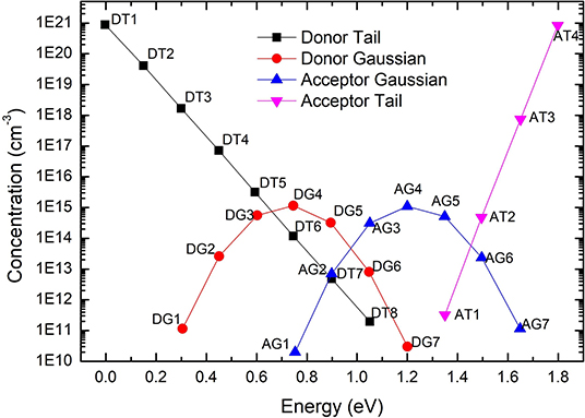
Figure 1. Defect density or concentration (without weighting factor) of conduction and valence band tail states and Gaussian states within the a-Si:H material.
Despite the significant differences within the structure of c-Si and a-Si:H, only a few parameters within the new “aSiH.par” material parameter file were required to be modified. Firstly, the electron and hole mobilities were adjusted from 1,417 and 470.5 cm2 V-1 s-1, to 10 and 0.01 cm2 V-1 s-1, respectively, in accordance with the relevant literature [2, 17]. The second major change to the material parameter file was the adjustment of the band-gap and is presented in the results, see Table 1. According to the literature, the band-gap of a-Si:H lies between 1.7 and 1.9 eV, depending on the hydrogen concentration and annealing temperature.
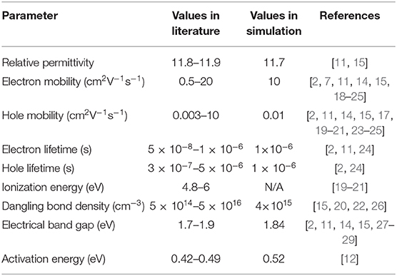
Table 1. Relevant criteria of the a-Si:H parameter file used in this study with comparison to values found in the literature.
2.2. The Physics Model
The Device Simulation for Smart Integrated Systems (DESSIS) tool kit native to Sentaurus TCAD solves the Poisson and electron/hole continuity equations in order to simulate the electrical behavior of the a-Si:H n-i-p device. The doping dependent Shockley-Read-Hall and trap assisted Auger physics models were activated to describe all carrier generation/recombination processes. The doping dependent, Enormal and high field saturation models were activated to describe the mobility of carriers within the simulation. The Poole-Frenkel model related to traps within the mid-gap was activated in order to take into account the enhanced emission probability (ΓPF) for charged trap centers, due to the reduction in the potential barrier associated with the presence of high external electric fields (E). As shown in Equation (1), the role of ΓPF is to adjust the initial trap cross sections from to their new value of as determined by the Poole-Frenkel trap model. The enhanced emission probability (see Equation 2) can be treated as a variable through the manipulation of the tuning parameter α (see Equation 3) via the adjustment of εPF from the default value of 11.7 [30]. It should be noted that k, T, and q in Equation (3) refer to Boltzmann's constant, temperature and electronic charge.
The Poole-Frenkel mobility model was originally designed in TCAD to simulate organic semiconductors for thin film transistors and photovoltaic devices and was considered in the early phases of this work, however, its inclusion was subsequently discontinued as it was deemed to be incompatible with the distribution of defects introduced with the defect-pool model of the DBs and thus its inability to correctly mimic the E-field () dependence upon the current density.
2.3. Geometry of the Device
In this study, we chose to model a simplified 2D version of the n-i-p (n-doped, intrinsic, and p-doped layers) a-Si:H diode structure as described by Wyrsch et al. [8]. The geometry depicted in Figure 2, features a 90 nm thick n-type layer upon a 30 μm thick intrinsic layer upon a 90 nm thick p-type layer. The intrinsic layer is simulated in two different thicknesses to evaluate the capability of the model to scale macroscopic characteristics such as leakage current, electric field distribution and charge collection efficiency with thickness appropriately. The p-type and n-type doped layers are modeled using a Gaussian analytic function with peak concentrations of 3 × 10+18 and 8 × 10+18 cm-3, respectively. The modeled device is 50 μm wide and given its 2D nature, is by default 1 μm deep.
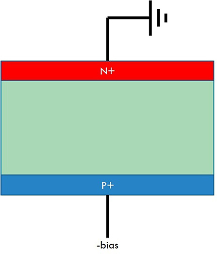
Figure 2. n-i-p structure of the a-Si:H diode. The n-type (red) and p-type (blue) layers are 90 nm thick and the intrinsic (green) layer is 30 μm thick.
Given that the model is a 2D representation of the a-Si:H n-i-p device, a geometric scaling factor AF was used to allow for a comparison between experimental and simulated leakage current density. This geometric scaling factor is used to account for the considerably different areas of the experimental (2 × 2 mm2) and simulated (50 × 1 μm2) device structures. A discretized meshing strategy was applied to the entire geometry in order to solve and evaluate the Poisson and electron/hole continuity equations throughout the geometry. As part of the meshing process, the doping dependent mesh strategy was employed to optimize the number of nodes in regions of interest to improve simulation accuracy and minimize computational time.
2.4. Simulation Process
After appropriate specification of the adjusted material parameters and defect distribution within the mid-gap, a preliminary steady-state simulation of the electrical behavior of the 30 μm thick a-Si:H n-i-p device was performed and compared to experimental results. The DC-simulation technique was used to investigate the leakage current of a 12 and a 30 μm thick device from 0 to 200 and 0 to 400 V, respectively. The same simulation set-up was used to investigate the electric field distribution as a function of bias for verification of the depletion region achievable in the intrinsic layer of the device. Lastly, the charge collection efficiency was evaluated by means of a transient simulation of a MIP with a linear energy transfer of 1.28 × 10⁻⁵ pC μm-1 traversing the center of the device.
3. Results and Discussion
3.1. Current-Voltage Characteristics
Because the band-gap of a-Si:H is dependent upon the concentration of introduced hydrogen. A preliminary study was performed to investigate the effect of the band-gap (1.70 eV ≤ Eg ≤ 1.90 eV) upon the simulated leakage current density and is depicted in Figure 3. In this study, the most appropriate value of the band-gap or Eg was determined to be 1.84 eV. The appropriateness of the value of Eg was determined by considering the agreement between the experimental and simulated leakage current density and is described in more detail below.
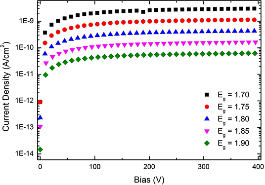
Figure 3. Simulated current density as a function of applied bias for a range of different band-gaps from 1.70 ≤ Eg ≤ 1.90.
Unique scaling factors were applied to the acceptor and donor defect states ATi, AGi, DGi, and DTi depicted in Figure 1, which are 0.001, 5, 1, and 0.001, respectively. The results of the leakage current simulation by means of a static DC simulation for the 12 and 30 μm thick a-Si:H n-i-p devices are presented in Figures 4, 5. A comparison of the simulated results with experimental results provided by Wyrsch et al. is made [8]. In both cases, the model employed was not able to mimic the experimental results satisfactorily. This discrepancy is a result of the transition from drift dominated transport to Poole-Frenkel transport with its well known square root of the electric field () dependency [31]. As the magnitude of the electric field increases, charge carriers trapped within defect centers are able to acquire sufficient energy to contribute to conduction within the device. To that end, a fitting function described by Equation (4), was employed to mimic the high field dependency of the experimental leakage current density (J). The aforementioned equation includes a modified version of the Poole-Frenkel effect which describes the dependency. Note in this equation, J0 is a dimensionality constant (A cm-2), E is the electric field strength (V cm-1), d is the substrate thickness in cm and JSRH is the current density simulated by TCAD, based upon Shockley-Read-Hall statistics, taking into account the temperature, electric field, effective carrier concentration, and generation-recombination centers. It should be noted that the Poole-Frenkel trap model previously discussed was investigated in this study. However, it was determined that its activation has no impact upon the results.
The summation (green circles) of the simulated current density (red circles) and the fitting function (blue triangles) provides excellent agreement with the experimental data (black squares) for both the 12 and 30 μm thick a-Si:H n-i-p devices (see Figures 4, 5). The result presented in a semi-log scale shows an agreement (within 10 nA cm-2) between the two data sets. The fitting parameters b and J0 are set to 2.5 × 10⁻⁴ cm0.25 V-0.5 and 5.5 × 10⁻¹³ A cm-2 for both the 12 and the 30 μm thick substrates, showing the capability of the model to scale the leakage current consistently with the thickness of the intrinsic layer maintaining good agreement with the experimental results. Similar to the ideality factor in the Shockley diode equation [32, 33], the fitting parameters b and J0 are to account for variations of the a-Si:H material quality and/or fabrication processes.
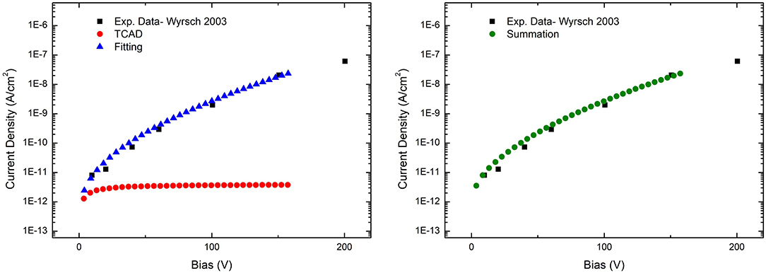
Figure 4. Comparison of experimental (black square) and simulated (red circle) current density characteristics as a function of externally applied bias for the 12 μm thick a-Si:H n-i-p device. A fitting function (Blue triangles) described by Equation (4) was employed to fit the field dependent components of the data. The summation of the simulated and fitted result (green circles) compared to the experimental result is presented on the right.
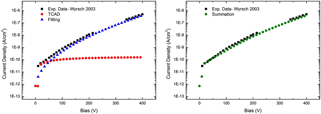
Figure 5. Comparison of experimental (black square) and simulated (red circle) current density characteristics as a function of externally applied bias for the 30 μm thick a-Si:H n-i-p device. A fitting function (Blue triangles) described by Equation (4) was employed to fit the field dependent components of the data. The summation of the simulated and fitted result (green circles) compared to the experimental is presented on the right.
3.2. Electric Field Distribution
The electric field is obtained from the gradient of the electrostatic potential. In this section the distribution of the electric field for the 12 and 30 μm thick a-Si:H n-i-p structures for different applied bias is investigated. Figure 6 depicts the cross section of the electric field distribution for the 12 and 30 μm thick a-Si:H n-i-p structures, respectively. The cross section is taken through the center of the device, i.e., x = 0, in order to show how the electric field changes with respect to diode thickness. The DC results of the 12 μm thick a-Si:H n-i-p structures show full depletion for applied bias between 48 and 96 V, corresponding to an electric field strength (EMag) with a magnitude of 4–8 V μm-1. Similarly, the DC results of the 30 μm thick a-Si:H n-i-p structures show full depletion for applied bias between 300 and 360 V (EMag=10–12 V μm-1). This quantitative analysis of the bias required to fully deplete the 12 and 30 μm thick a-Si:H n-i-p structures is crucial in terms of understanding the operating conditions required to operate such devices for detection of single ionizing radiation events.
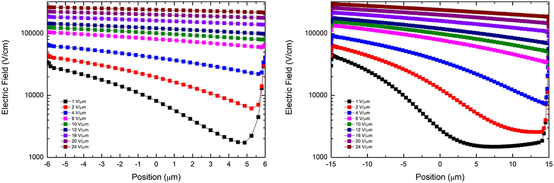
Figure 6. Simulated distribution of the electric field within the 12 μm thick n-i-p a-Si:H diode (left) and the 30 μm thick n-i-p a-Si:H diode (right) as a cross section of the electric field distribution in the same device.
3.3. Charge Collection Study
The “HeavyIon” model native to Sentaurus TCAD was adapted to mimic a MIP traversing the 12 μm thick a-Si:H n-i-p devices at specific time (t0 = 10 ns) and location (x = 0). The Linear Energy Transfer (LET) for the MIP was set to 1.28 × 10⁻⁵ pC μm-1 corresponding to approximately 80 pairs.μm-1. As shown previously, the large concentration of traps is associated with a large leakage current density. It also leads to substantial instability in the transient behavior of the material. In order to calculate the charge collection associated with the ion strike, the transient instability must be taken into account. Figure 7 (left) depicts the transient behavior of the 12 μm thick a-Si:H substrate due to a MIP strike under an applied bias of 96 V after subtraction of the baseline leakage current without the MIP. Using this result, the Charge Collection Efficiency (CCE) is assessed by considering the integral of the current over a time window of 3 ns and is normalized with respect to the maximum CCE observed. The CCE as a function of the square root of the applied bias for the 12 μm thick a-Si:H n-i-p devices is presented in Figure 8. In order to assess the functionality of the Poole-Frenkel trap model, the simulation was performed with and without the model activated as shown in Figure 8.
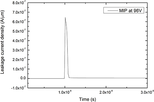
Figure 7. MIP strike within the 12 μm thick a-Si:H substrate at t0=10 ns under an applied bias of 96 V. This result takes into account the time sensitive behavior of the leakage current. The integral of the transient response is used to assess the charge collection associated with the MIP strike.
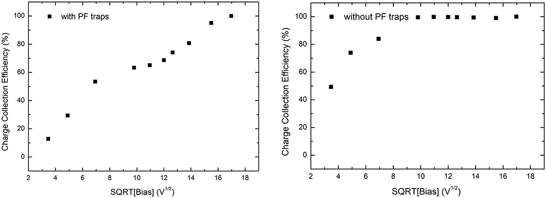
Figure 8. CCE vs. for the 12 μm thick a-Si:H n-i-p device. Simulations were run with (left) and without (right) the Poole-Frenkel trap model activated.
Although the simulated CCE behavior with the Poole-Frenkel trap model activated shows a predictable trend at lower biases, it displays a significant deviation from the expected behavior at higher biases, with obvious non-linear trend and lack of CCE saturation indicating that the model is not presently capable of modeling the depletion of thick a-Si:H substrates. In contrast, the simulated CCE behavior without the Poole-Frenkel trap model activated manifests the expected trend with a linear increase in CCE at lower biases and saturation in the condition of over-depletion. At low biases, the CCE is hampered by the defects within the a-Si:H material limiting charge collection through trapping processes and reduction of the carrier mean free path. Once the bias is increased sufficiently, there is an increased proportion of charge carriers able to contribute to the current, until such point that the charge collection saturates.
Using the CCE behavior without the Poole-Frenkel trap model, allows an alternative method of determining the operating conditions required to fully deplete the device in order to measure the signal due to incident ionizing radiation. Plotting two linear fitting functions to the CCE behavior, one in the low bias region and the second in the high bias region where the charge collection has saturated, allows determination of the point at which these lines intersect. Determination of the intersection position on the x-axis, i.e., the square root of the bias, gives a rough approximation of the depletion voltage. Using this method, a voltage of 68 ± 20 V is given, corresponding to an electric field strength of 5.7 V μm-1. Despeisse et al. [12] and Wyrsch et al. [34] provides an empirically based formalism to predict the depletion voltage (VD) of a-Si:H based devices with DB density of the order of 1014 using only the device thickness in μm (D), i.e., VD ≈ 0.48 × D2. According to this formalism, the substitution of our device thickness of 12 μm gives a depletion voltage of 69 V, corresponding to electric field strengths of 5.75 V μm-1. In the case of the 12 μm thick device, the two methods provide excellent agreement (≈1%) in terms of the prediction of the depletion voltage. This is in agreement with the result predicted by the DC simulation which depicts the electric field strength as a function of depth within the a-Si:H substrate and predicts depletion for electric field strengths between 4 and 8 V μm-1 for the 12 μm thick device.
Applying the same methodology to the data set obtained for the 30 μm thick device (see Figure 9), the depletion voltage, as determined by the CCE as a function of the the square root of the bias, is determined to be 300 ± 30 V, corresponding to an electric field strength of 10 V μm-1. This result fits with the earlier prediction of depletion occurring between 300 and 360 V based upon the electric field distribution. In comparison, the depletion voltage obtained by the formalism proposed by Despeisse shows a discrepancy of approximately 20%, corresponding to an electric field strength of 14.4 V μm-1.
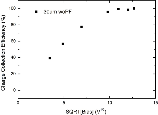
Figure 9. CCE vs. sqrt(V) for the 30 μm thick a-Si:H n-i-p device without activation of the Poole-Frenkel trap model.
4. Discussion and Conclusion
Amorphous silicon technology presents several advantages for the development of ionizing radiation detectors: it allows deposition over flexible materials such as plastics; it can be easily patterned creating pixellated large area detectors; it has an intrinsically high radiation hardness associated with its high degree of native disorder. For these reasons, a tool capable of optimizing the design of radiation detector geometries based on a-Si:H is desirable. In this study, a new material model to mimic the electrical and charge collection behavior of a-Si:H has been developed using the Sentaurus TCAD suite. Two a-Si:H based device structures, identical with the exception of their thickness (12 and 30 μm) were modeled. In order to model the highly disordered structure of an a-Si:H substrate, multiple acceptor/donor defects characteristic of the quasi-continuous conduction/valence tail states and the Gaussian mid-gap states have been introduced.
The use of a commercially available TCAD suite, largely diffused in the radiation detection scientific community, presents some advantages to develop a model for a radiation detector: the model is portable, reproducible and expandable to include further properties or parameters in the simulation of the device. A limitation associated with this strategy is the use of models which may not be developed specifically for the material adopted. At present, TCAD doesn't have a library for a-Si:H and none of the models associated with Poole-Frenkel transport have been optimized for this specific material. Because of this limitation, the leakage current density simulated as a function of the applied potential was unable to mimic the experimental behavior without application of a fitting function featuring the square-root of the electric field dependency associated with Poole-Frenkel transport in a-Si:H. Regardless, the model has demonstrated capability of determining the operating conditions, i.e., the bias required for depletion, of a-Si:H based devices. The static DC simulations were used to show the electric field distribution as a function of position through the thickness of the 12 and 30 μm devices. The model was able to show that an operational voltage for the 12 μm thick device between 48 and 96 V corresponding to an electric field strength of 4–8 V μm-1 was required to fully deplete the device; an obvious necessity considering the context of operating as a sensor for ionizing events. Likewise, the model of the 30 μm predicts an operational voltage between 300 and 360 V, corresponding to an electric field strength of 10–12 V μm-1 to fully deplete the device. A previous study by De Greef et al. proved that a model based on the combination of SRH statistics and amphoteric behavior of the defects is effective in modeling the behavior of aSi:H [35]. Whilst they did not investigate the effect of high electric fields on the dark reverse current, they proved that at low bias, recombination is the dominant source of leakage current while at high temperatures (equivalent to a high electric field condition) the formalism of amphoteric states becomes more significant. This result confirms our finding where the current density calculated by TCAD using the SRH statistics is significant only at low bias while it is dominated at high voltages by emission associated with tail states described by the Poole-Frenkel effect. The model discussed by De Greef et al. [35] calculates with great accuracy all the effects on current density due to temperature, density and spatial distribution of the defects in a device with uni-dimensional geometry (using the software D-AMPS). The Synopsys TCAD model developed in this study does not currently provide the same accuracy of the model developed in D-AMPS due to the limitations of the numerical models already embedded in the commercial tool. However, Synopsys TCAD provides the means to tune the models to achieve an acceptable accuracy. Furthermore, it provides the additional advantage of simulating 2D or even 3D models of the device. This feature allows having a better understanding of the effects on electric field distribution and on the charge collection efficiency created by specific geometries, relative position and dimensions of the electrodes which is of paramount importance for fine tuning of a position sensitive ionizing radiation detector. Transient analysis of MIPs was performed with and without activation of the Poole-Frenkel trap model for the 12 μm thick a-Si:H device structure. The results derived from the simulation with the Poole-Frenkel trap model activated depict behavior that is at odds with what has been shown experimentally within the literature [8], and so the Poole-Frenkel trap model in its current implementation is deemed to be incompatible with thick a-Si:H substrates. Conversely, the results derived from the simulation without activation of the Poole-Frenkel trap model depict the expected charge collection behavior of a device before and after being fully depleted. Analysis of the aforementioned results gives a depletion voltage of 68 ± 20 V which is within 1% of that predicted by the formalism provide by Despeisse et al. [12] of 69 V. The depletion voltage obtained from the CCE as a function of the square root of the applied bias for the 30 μm thick substrate is 300 ± 30 V, which differs from the formalism of Despeisse by approximately 20%. The model underestimates the depletion voltage in thick devices in comparison with the results obtained by experimental methods because a thicker substrate presents larger probability to have a different degree of disorder across the intrinsic layer, requiring a larger voltage to be depleted. Such behavior can be taken into account by creating successive layers of substrate with increasing concentration of tail states. The good agreement between the simulated charge collection and the aforementioned requirements to fully deplete the device indicate the suitability of the TCAD modeling approach as a predictive tool for the design and optimization of a-Si:H radiation detectors. It should be noted that the determination of depletion voltage via the charge collection efficiency as a function of voltage is not the standard method and should only be treated as an approximation. Thus the next step in this work will be to utilize the small-signal analysis simulation method, whereby the capacitance of the a-Si:H devices as a function of bias may be determined. Future work in this area will focus upon optimization of device geometries for particle detection, including charge sharing, inter-pixel capacitance, and electric field distribution, as well as continued development of the model in terms of radiation damage upon the effects and variation of the CC and depletion as a function of the temperature. In addition, the Sentaurus Physical Model Interface (PMI) will be investigated as a means of implementing modifications to the existing Poole-Frenkel mobility model to be applicable for thick a-Si:H substrates in order to improve the robustness of the numerical model.
Data Availability Statement
A detailed list of the energy states included in the simulations is included in the Supplementary Material.
Author Contributions
JD, BT, and MP contributed equally to the conduction of all simulations. ML assisted with the data analysis of the J-V characteristics of the simulation data. All other authors contributed to discussion of the results and the write-up of the manuscript.
Funding
This study is part of the project 3D-SiAm, funded by the National Commission 5 of the Istituto Nazionale di Fisica Nucleare—Italy.
Conflict of Interest
The authors declare that the research was conducted in the absence of any commercial or financial relationships that could be construed as a potential conflict of interest.
Supplementary Material
The Supplementary Material for this article can be found online at: https://www.frontiersin.org/articles/10.3389/fphy.2020.00158/full#supplementary-material
References
1. Bora B, Sastry O, Kumar A, Dahiya R, Bangar M, Prasad B. Estimation of most frequent conditions and performance evaluation of three photovoltaic technology modules. J Solar Energ Eng. (2016) 138:054504. doi: 10.1115/1.4034202
2. Nawaz M. Design analysis of a-Si/c-Si HIT solar cells. Adv Sci Technol. (2010) 74:131–6. doi: 10.4028/www.scientific.net/AST.74.131
3. Bourland JD. Clinical Radiation Oncology. Elsevier (2016). Available online at: https://linkinghub.elsevier.com/retrieve/pii/C20130006482 (accessed February 25, 2020).
4. Ducourant T, Wirth T, Bacher G, Bosset B, Vignolle J, Blanchon D, et al. Latest advancements in state-of-the-art aSi-based x-ray flat panel detectors. In: Proceedings SPIE, Medical Imaging 2018: Physics of Medical Imaging. Houston, TX (2018). p. 10573. doi: 10.1117/12.2291908
5. Brace OJ, Alhujaili S, Deshpande S, Davis JA, Vial P, Metcalfe P, et al. Feasibility of a dual detector system to perform transit dosimetry and MV imaging in-vivo. J Instrumen. (2019) 14:P01019. doi: 10.1088/1748-0221/14/01/P01019
6. Fortunato E, Pereira L, Aguas H, Ferreira I, Martins R. Flexible a-Si:H position-sensitive detectors. Proc IEEE. (2005) 93:1281–6. doi: 10.1109/JPROC.2005.850302
7. Despeisse M, Jarron P, Johansen KM, Moraes D, Shah A, Wyrsch N. Preliminary radiation tests of 32-m thick hydrogenated amorphous silicon films. Nucl Instrum Methods Phys Res Sect A. (2005) 552:88–92. doi: 10.1016/j.nima.2005.06.012
8. Wyrsch N, Ballif C. Review of amorphous silicon based particle detectors: the quest for single particle detection. Semiconduct Sci Technol. (2016) 31:103005. doi: 10.1088/0268-1242/31/10/103005
9. Winer K. Defect pool model of defect formation in a-Si:H. J Non-Crystall Solids. (1991) 137:157–62. doi: 10.1016/S0022-3093(05)80080-8
10. Movaghar B, Grünewald M, Pohlmann B, Würtz D, Schirmacher W. Theory of hopping and multiple-trapping transport in disordered systems. J Stat Phys. (1983) 30:315–34. doi: 10.1007/BF01012306
11. Dutta U, Chatterjee P. The open circuit voltage in amorphous silicon p-i-n solar cells and its relationship to material, device and dark diode parameters. J Appl Phys. (2004) 96:2261–71. doi: 10.1063/1.1769092
12. Despeisse M, Anelli G, Jarron P, Kaplon J, Moraes D, Nardulli A, et al. Hydrogenated amorphous silicon sensor deposited on integrated circuit for radiation detection. IEEE Trans Nucl Sci. (2008) 55:802–11. doi: 10.1109/TNS.2008.918519
13. Synopsys TCAD. Synopsys. (2013). Available online at: https://www.synopsys.com/silicon/tcad.html (accessed February 25, 2020).
14. Lee C, Efstathiadis H, Raynolds JE, Haldar P. Two-dimensional computer modelling of single junction a-Si:H solar cells. In: 2009 34th IEEE Photovoltaic Specialists Conference (PVSC). Philadelphia, PA (2009). p. 001118–22. doi: 10.1109/PVSC.2009.5411215
15. Otero P, Rodriguez JA, Vetter M, Andreu J, Comesa na E, Garcia Loureiro A. Simulation of the temperature dependence of a-Si:H solar cell current-voltage characteristics. In: Spanish Conference on Electron Devices. Palma de Mallorca (2011). p. 1–4. doi: 10.1109/SCED.2011.5744227
16. Petasecca M, Moscatelli F, Passeri D, Pignatel GU. Numerical simulation of radiation damage effects in p-type and n-type FZ silicon detectors. IEEE Trans Nucl Sci. (2006) 53:2971–6. doi: 10.1109/TNS.2006.881910
17. Despeisse M, Anelli G, Commichau S, Dissertori G, Garrigos A, Jarron P, et al. Characterization of 13 and 30-m thick hydrogenated amorphous silicon diodes deposited over CMOS integrated circuits for particle detection application. Nucl Instrum Methods Phys Res Sect A. (2004) 518:357–61. doi: 10.1016/j.nima.2003.11.022
18. Xi J, Hollingsworth RE, Buitrago RH, Oakley D, Cumalat JP, Nauenberg U, et al. Minimum ionizing particle detection using amorphous silicon diodes. Nucl Instrum Methods Phys Res Sect A. (1991) 301:219–22. doi: 10.1016/0168-9002(91)90462-Y
19. Equer B, Karar A. Effect of primary ionization in amorphous silicon detectors. Nucl Instrum Methods Phys Res Sect A. (1988) 271:574–84. doi: 10.1016/0168-9002(88)90324-5
20. Perez-Mendez V, Kaplan SN, Cho G, Fujieda I, Qureshi S, Ward W, et al. Hydrogenated amorphous silicon pixel detectors for minimum ionizing particles. Nucl Instrum Methods Phys Res Sect A. (1988) 273:127–34. doi: 10.1016/0168-9002(88)90807-8
21. Perez-Mendez V, Cho G, Drewey J, Jing T, Kaplan SN, Mireshghi A, et al. Amorphous silicon pixel radiation detectors and associated thin film transistor electronics readout. Nucl Phys B. (1993) 32:287–95. doi: 10.1016/0920-5632(93)90036-6
22. Anelli G, Commichau SC, Despeisse M, Dissertori G, Jarron P, Miazza C, et al. A new concept of monolithic silicon pixel detectors: Hydrogenated amorphous silicon on ASIC. Nucl Instrum Methods Phys Res Sect A. (2004) 518:366–72. doi: 10.1016/j.nima.2003.11.024
23. Qureshi S, Perez-Mendez V, Kaplan SN, Fujieda I, Cho G, Street RA. Signal generation in a hydrogenated amorphous silicon detector. IEEE Trans Nucl Sci. (1989) 36:194–8. doi: 10.1109/23.34433
24. Hong WS, Drewery JS, Jing T, Lee H, Kaplan SN, Perez-Mendez V, et al. Charged particle detectors based on high quality amorphous silicon deposited with hydrogen or helium dilution of silane. IEEE Trans Nucl Sci. (1995) 42:240–6. doi: 10.1109/23.467843
25. Dubeau J, Pochet T, Hamel LA, Equer B, Karar A. Response of amorphous silicon p-i-n detectors to ionizing particles. Nucl Instrum Methods Phys Res Sect B. (1991) 54:458–71. doi: 10.1016/0168-583X(91)95394-S
26. Mireshghi A, Cho G, Drewery JS, Hong WS, Jing T, Lee H, et al. High efficiency neutron sensitive amorphous silicon pixel detectors. IEEE Trans Nucl Sci. (1994) 41:915–21. doi: 10.1109/23.322831
27. Hasegawa S, Yazaki S, Shimizu T. Effects of annealing on gap states in amorphous Si films. Solid State Commun. (1978) 26:407–10. doi: 10.1016/0038-1098(78)90515-X
28. Vaněček M, Stuchlík J, Kočka J, Tříska A. Determination of the mobility gap in amorphous silicon from a low temperature photoconductivity measurement. J Non-Crystall Solids. (1985) 77–8:299–302. doi: 10.1016/0022-3093(85)90660-X
29. Omer B, Mohammed FA, ASAM. Simulation study on the open-circuit voltage of amorphous silicon p-i-n solar cells using AMPS-1D. J Nano Electron Phys. (2014) 6:1–4.
30. Colalongo L, Valdinoci M, Baccarani G, Migliorato P, Tallarida G, Reita C. Numerical analysis of poly-TFTs under off conditions. Solid State Electron. (1997) 41:627–33. doi: 10.1016/S0038-1101(96)00201-8
31. Frenkel J. On pre-breakdown phenomena in insulators and electronic semi-conductors. Phys Rev. (1938) 54:647–8. doi: 10.1103/PhysRev.54.647
32. Shockley W. The theory of p-n junctions in semiconductors and p-n junction transistors. Bell Syst Techn J. (1949) 28:435–89. doi: 10.1002/j.1538-7305.1949.tb03645.x
33. Mao LF. Physical origins of the ideality factor of the current equation in Schottky junctions. Pramana J Phys. (2020) 94:16. doi: 10.1007/s12043-019-1868-2
34. Wyrsch N, Miazza C, Dunand S, Shah A, Blanc N, Kaufmann R, et al. Development of vertically integrated imaging and particle sensors. In: Materials Research Society Symposium - Proceedings. San Francisco, CA (2003). p. 762. doi: 10.1557/PROC-762-A18.14
Keywords: a-Si:H, radiation hardness, large area application, radiation sensor, high energy physics
Citation: Davis JA, Boscardin M, Crivellari M, Fanò L, Large M, Menichelli M, Morozzi A, Moscatelli F, Movileanu-Ionica M, Passeri D, Petasecca M, Piccini M, Rossi A, Scorzoni A, Thompson B, Verzellesi G and Wyrsch N (2020) Modeling a Thick Hydrogenated Amorphous Silicon Substrate for Ionizing Radiation Detectors. Front. Phys. 8:158. doi: 10.3389/fphy.2020.00158
Received: 17 September 2019; Accepted: 16 April 2020;
Published: 08 May 2020.
Edited by:
Paul Sellin, University of Surrey, United KingdomReviewed by:
Konstantin Stefanov, The Open University, United KingdomPeter R. Hobson, Queen Mary University of London, United Kingdom
Copyright © 2020 Davis, Boscardin, Crivellari, Fanò, Large, Menichelli, Morozzi, Moscatelli, Movileanu-Ionica, Passeri, Petasecca, Piccini, Rossi, Scorzoni, Thompson, Verzellesi and Wyrsch. This is an open-access article distributed under the terms of the Creative Commons Attribution License (CC BY). The use, distribution or reproduction in other forums is permitted, provided the original author(s) and the copyright owner(s) are credited and that the original publication in this journal is cited, in accordance with accepted academic practice. No use, distribution or reproduction is permitted which does not comply with these terms.
*Correspondence: Marco Petasecca, bWFyY29wJiN4MDAwNDA7dW93LmVkdS5hdQ==