
94% of researchers rate our articles as excellent or good
Learn more about the work of our research integrity team to safeguard the quality of each article we publish.
Find out more
ORIGINAL RESEARCH article
Front. Phys. , 18 March 2020
Sec. Optics and Photonics
Volume 8 - 2020 | https://doi.org/10.3389/fphy.2020.00052
This article is part of the Research Topic Nonlinear Photonics View all 6 articles
 Nassima Benchtaber*
 Abdelhakim Nafidi
 Driss Barkissy
 Abderrezak Boutramine
 Merieme Benaadad
 Samir Melkoud
 Es-Said Es-Salhi
 Fatiha Chibane
We have used the envelope function formalism to investigate the bands structure of LWIR type II SL InAs (d1 = 2. 18d2)/In0.25Ga0.75Sb(d2 = 21.5 Å). Thus, we extracted optical and transport parameters as the band gap, cut off wavelength, carriers effective mass, Fermi level and the density of state. Our results show that the higher optical cut-off wavelength can be achieved with smaller layer thicknesses. The semiconductor-semi metal transition was studied as a function of temperature. Our results permit us the interpretations of Hall and Shubnikov-de Haas effects. These results are in agreement with experimental results in literature and a guide for engineering infrared detectors.
There are a several efforts in developing infrared materials for Very Long Wavelength Infrared (VLWIR) photodetection with the optical cut-off wavelengths λc ≥ 7.5 μm in the atmospheric window. Currently, InAs/In1−xGaxSb type-II superlattices (SLs) are still the most promising candidate. In this area, Smith and Mailhiot [1] have shown that this material system provides distinctive advantages suitable for VLWIR photodetection.
The key lies in the fact that by increasing indium composition in In1−xGaxSb layer, the corresponding lattice constant increases. As a result, the tension in the InAs layer lowers the conduction subbands (Ei) whereas the compression in the In1−xGaxSb layer raises the heavy hole subband (HHi). Therefore, a very smaller band gap can be optimized with a reasonably thinner period which is not possible in InAs/GaSb SL [2]. The most important advantage of this SL lies in the fact that the presence of strain within this SL layers reduces the Auger recombination process and improves significantly the carrier lifetime and detectivity [3]. We note that in the previous years, a very few works were reported to verify the theoretical performance of InAs/InGaSb SLs for LWIR and VLWIR photodetection.
The applications of this technology are in military, automobile, aircraft safety, medical diagnosis, and in remote sensing systems [4].
The theory of band structure is necessary for describing the effects of external excitations on transport parameters and properties of optoelectronics devices [5]. Owing to this lack of studies, we have investigated the bands structure of presented LWIR type II SL InAs (d1 = 47 Å)/Ga0.75In0.25Sb(d2 = 21.5 Å) with d1/d2 = 2.186 along the wave vector kz in the growth direction and kp(kx,ky) in-plane of the superlattice. We extracted useful electro-optical parameters like the optical cut-off wavelength, the effective mass of electrons and holes and their evolution with temperature. We found the point of semiconductor (SC) to Semimetal (SM) transition. We calculated the density of states without and with applied magnetic field and deduced the dimensionality and the limit of the quantification of the energy of electron gas.
The general expression of dispersion relation of type-II SLs, within the envelope function formalism and effective mass approximation, is given by [6–9]:
In each host material, we used the six bands Kane Hamiltonian (6*6 matrix) describing the k.p interaction of Γ6 doublet for electrons) and Γ8 quadruplet for light holes and for heavy holes]. The spin-orbit coupling is too large, compared to the hosts gaps εi, so the Γ7 doublet is neglected. With the help of the Bloch condition, the continuity of the envelope functions and their derivatives at the interfaces we obtain a system with solution Equation (1). The inferior limit of the validity of this model is d1 < 10 Å and d2 <10 Å as indicated by Bastard [6], Andlauer and Vog [7], Masur et al. [8]. Here kz and kp(kx,ky) are the wave vector in the growth direction and in-plane of the superlattice. The origin of the energy E has been chosen at the top of InAs valence band as shown in the Figure 1. In each host material and for a given energy, the two–band Kane model [10] gives the wave vector (+ ). Therefore, the energy E of the light particles (electron and light hole) is given by:
The expression of ξ and r in the Equation (1) are:
From the same Equation (1), the superlattice heavy holes mini-bands can be calculated with the following relations:
The direct band gaps parameters εi (i = 1 and 2) used here, as a function of temperature, are given by the empirical expressions reported in Matossi and Stern [11] and Roth et al. [12]. Pi is the Kane matrix element.
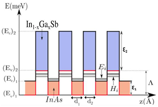
Figure 1. Energy bands alignment in InAs/In1−xGaxSb SL along the growth axis z. (Ec)i, (Ev)i, and ϵi where i = 1 and 2 are conduction and valence band edges and band gap of bulks, respectively. ΔEv = ∧ is the valence band offset.
The heavy holes effective masses of InAs and In0.25Ga0.75Sb are, respectively ()1= 0.41 m0 and ()2 = 0.42 m0, as given in Levinshtein et al. [13]. Here m0 is the free electron mass.
In this work, we have used the valence band offset Λ of 510 meV between heavy holes sub-bands edges of InAs and In0.25Ga0.75Sb [14]. The origin of energy is taken on the top of VB in InAs (Figure 1).
The computation of band structures consists of solving the general dispersion relation with the reported parameters. In the Equation (1), state energy exists if the right-hand side lies in the range −1 to 1. In other words, −1 ≤ cos (kz d) ≤ 1 which implies –π/d ≤ kz ≤ π/d in the first Brillouin zone, with d = d1+d2 is the superlattice period. In the study of energy E as a function of wave vector in the direction of growth kz (kp = 0), the solving procedure consists of going with small steps of energy through the studied range. Then finding, for a given E, the value of kz which is root of the dispersion relations. The same procedure is used for studying E vs. the in-plane wave vector kp (kz = 0 and kz = π/d).
In the Figure 2, we have plotted the energy of conduction (Ei), light-hole (hi), and heavy-hole (HHi) subbands at the center Γ(kz = 0) and the limit (kz = π/d) of the first Brillouin zone (FBZ) as a function of d1 = 2.18 d2 at 1.2 K. These results show that when d1 increases, the width of Ei and HHi deceases. In addition, we can notice that the fundamental band gap energy Eg(Γ) = E1(Γ)–HH1(Γ) decreases when d1 increases. Therefore, a crossover between E1 and HH1 takes place at the semiconductor (SC) to Semimetal (SM) transition point Tc(d1c = 115.43 Å, E1c = HH1c = 485.25 meV).
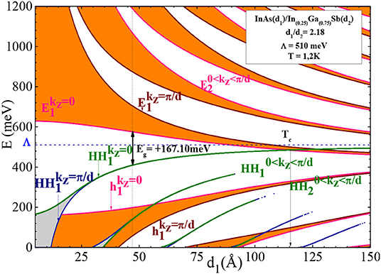
Figure 2. Energy position and width of Ei, HHi and hi subbands calculated at 1.2 K, in the FBZ as a function of d1.
In Figure 3, at a given temperature the Eg decreases when the valence band offset ∧, between the top of the heavy hole bands in the two host materials, increases. The transition SC-SM occurs when Eg goes to zero.
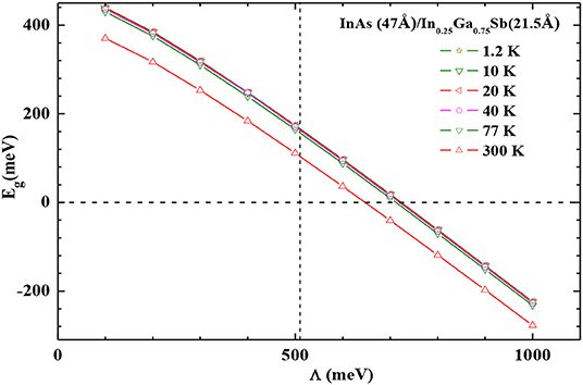
Figure 3. Band gap, Eg, as a function of the valence band offset at different temperatures in the investigated superlattice. The vertical dashed line indicates our chosen value of 510 meV.
The evolution of the cut off wavelength |λc| as a function of d2 is shown in Figure 4. These results were calculated by using the expression:
The dependencies of |λc(Γ)| on d2 and temperature (T) are shown in Figure 4. The figure divides itself into two regimes: (i) For d2 ≤ d2c: for each T, λc(Γ, d2) increases significantly with increasing d2. When d2 exceeds the critical value of d2c, E1 is confounded with HH1 at the SC-SM transition point where λc(Γ, d2c) diverges. The critical d2c decreases from 53.5 Å at 1.2 K to 37 Å at 300 K. Thus, the SC-SM transition goes to lower d1 when T increases. (ii) For d2 > d2c: E1 falls completely below HH1 and the SL shows an inverted bands structure with a SM conductivity. In this regime a reverse behavior was observed. The inset figure shows the sensitivity of Eg on T. This result shows that when T increases Eg shifts to lower energies with 0.21 meV/K. This is due to the fact that the thermal energy and electron-phonon interaction increase with T which lead to a reduction of the potential seen by electrons, leading to a reduced Eg. In the investigated temperature range, the corresponding 7.46 ≤ λc(μm) ≤ 11.94 situates this sample in the LWIR region. The SL bands structure shown in Figure 5 was computed at 1.2 K along kz and kp the growth and in-plan directions, respectively. Along kz, the widths of E1 and E2, |Ei(kz = π /d)– Ei(kz=0)|, were found to be 129 and 193 meV, respectively. The presence of such dispersion indicates three dimensional like behavior of electrons which is in agreement with the reported results of Mitchel et al. [15].
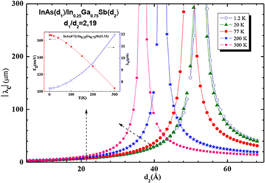
Figure 4. SLs |λc(Γ)| as a function of d2 for various temperatures. In the insert the variation of Eg(T) and λc(T) with temperature in the investigated SL.
The energy as a function of and at 1.2 K shows that: along kz, the bands Ei and hi of the light particles are non-parabolic and the heavy holes bands HHi are parabolic; but along kp, E1 and HHi are parabolic but h1 is non-parabolic. The theoretical effective mass in general turns out to be a tensor with nine components defined as [16]:
From Figure 5 we calculated carrier's effective mass of light particles: electrons E1, light holes h1 and heavy holes HH1, in the direction of growth (kz) and in plane (kp) of this sample. Figure 6 shows that along kp, (kp) = −0.41 m0 whereas (kp) increases from 0.092 m0 to 0.151 m0 and (kp) decreases from −0.026 to −0.339 m0 at kp = π/d. Along kz, (kz) and (kz) diverge at inflection points kz = 0.0269 Å−1 and kz = 0.103 Å−1, respectively. At these points the effective mass changes its sign, in electron and light-hole bands. The dashed vertical line indicate the (kp) = 0.0887 m0 at the Fermi wave vector kF. Rogalski [17] gives a larger electron effective mass m*/mo ≈ 0.02–0.03 in InAs/GaInSb SLs, compared to m*/mo = 0.009 in HgCdTe alloy with the same bandgap Eg ≈ 100 meV. These values are indicated without d1, d2, temperature and direction of the effective mass tensor. Our results at the center Γ of the first Brillouin zone are (kp) = 0.092 m0, (kz) = 0.026 m0, (kp) = (kz) = −0.026 m0, and (kp) = −0.41 m0.
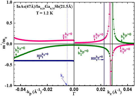
Figure 6. Calculated carrier's effective mass along the growth direction and in plan of the investigated SL.
We used the carrier density n as a function of the inverse of temperature measured in Mitchel et al. [18] and Haugan et al. [19]. In order to determine the band gap with accuracy, we plotted nT−3/2 as a function of 1,000/T. This lead to an experimental band gap of Eg= (95 ± 8) meV in the intrinsic domain, which is in agreement with our 104 meV calculated at 300 K. The observed difference of 8.87 meV is due to the reduction of the gap by strain [1] and the input parameters considered here as well as fluctuations during the growth of SL which could affect Eg. Note that Szmulowicz [20] and Szmulowicz et al. [21, 22] have studied the band structures of InAs(d1 = 43.6 Å)/In0.23Ga0.77Sb(d2 = 17.3 Å) with d1/d2 = 2.52 and the origin of energy taken at the bottom of the conduction band in InAs. The InAs conduction band–GaSb valence-band overlap was taken to be 140 meV. The band gap in this structure was tailored to be 120 meV. Whereas, Mitchel et al. [15] told a calculated Eg = 66.4 meV for this same sample. It's a contradiction and in addition the temperature of calculation of the gap was not given. From carrier density vs. inverse of temperature [18, 19], we deduced the activation energy Ea-Eg = 0.196 meV at low temperatures in agreement with the magnitude of thermal activation energy kBT at 2.3 K.
We plot the measured mobility μ in Mitchel et al. [18] and Haugan et al. [19] vs. temperature in logarithmic scales. This shows that when T increases, μ decreases as T−1.5 indicating the interaction of electrons with phonons in the intrinsic regime. This result confirms a tridimensional electron gas.
For the superlattice ith mini-band, with energy width ΔE(i) = E(i)max–E(i)min, the density of states (DOS) can be expressed as [23]:
The generalization of Equation (6) required a sum over all mini-bands:
From the dispersion curves E(kz) in Figure 5, we have calculated the SL density of states (DOS) of the two lowest conduction minibands Ei and the first valence subband HH1 at 1.2 K. As seen in Figure 7, the DOS is quantized in term of m*/πℏ2d, with the presence of large dispersion in Ei. This shows a significant interaction between InAs wells justified by the ratio d1 = 2.18 d2 in this sample.
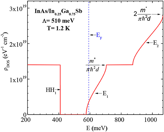
Figure 7. The SL DOS of the three subbands HH1, E1, and E2 at 1.2 K. The vertical dashed line indicates the position of the Fermi level energy EF.
At given temperature the Fermi level energy was obtained by the formula:
where and are the two dimensional and three dimensional Fermi wave vector, respectively and n is the measured concentration of carrier charge in the n(T) type sample [18, 19]. The effective masse of electrons at the Fermi wave vector kF is (kF) = 0.0887 m0 from Figure 6. The formula (8) permit as the determination of EF, at the center Γ of the first Brillouin zone, where all the bands are parabolic as seen in Figure 5.
In Figure 7, the calculated Fermi level energy EF is on the large E1 band indicating an n type (in agreement with [18, 19]) and quasi-bidimensional (Q2D) conduction behavior. Whereas, the full first valence subband HH1 has a very narrow band width indicating 2D-like behavior. The observation of Mitchel et al. [15] indicated a tridimensional conduction (3D).
In order to precise the dimensionality of carriers charges we plot, Figure 8 which shows the energy bands of light (h1), heavy (HH1) holes, and E1 electrons as a function of temperature. As can be seen, the band gap E1-HH1 decreases as the temperature increases. The Fermi level EF(3D) decreases with E1 when T increases. This is the behavior of a three-dimensional electron gas. For a two-dimensional electron gas the energy of Fermi level EF(2D) is constant i.e., independent of temperature as seen on the top of Figure 8. One can argue that the electron gas is Q2D up to Tc = 40 K and 3D for T ≥ Tc. We are witnessing a Q2D to 3D transition. In the following, we will consider that the electron gas is three-dimensional at temperature domain under consideration.
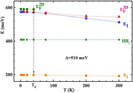
Figure 8. Energy of the first conduction (E1), valence (HH1 and h1) subbands, two and three dimensional Fermi level energy (EF) at different temperatures.
In the Mitchel et al. [18], Haugan, et al. [19], Szmulowicz [20], and Szmulowicz et al. [21, 22] the conduction bands E1 and E2 widths were ΔE1 = E1(kz = π/d)–E1(kz = 0) = 136.2 meV and ΔE2 = E2(kz = 0)–E2(kz = π/d) = 183.3 meV, respectively, with a separation between them ΔE(kz = π/d) = E2-E1 = 232.5 meV in the sample InAs(d1 = 43.6 Å)/In0.23Ga0.77Sb(d2 = 17.3 Å) with d1/d2 = 2.52. The width of HH1 was 0.01 meV along kz. Whereas, at 1.2 K, our calculated bands structure indicated Eg = 166.3 meV, ΔE1 = 123 meV, ΔE2 = 193 meV, and ΔE(kz = π/d) = 169.4 meV. The widths of HH1 are 0.05 meV and 20.8 meV along kz and kp, respectively. The band HH1 is flat along kz in Figures 1, 5 along q = kz in Szmulowicz [20] and Szmulowicz et al. [21, 22]. These values are in the same range as those given by Mitchel et al. [18], Haugan, et al. [19], Szmulowicz [20], and Szmulowicz et al. [21, 22] except for the band gap given there without temperature.
We have calculated the Fermi level in this SL by using the magnetoresistance results reported in Mitchel et al. [15].
It is well-known that the oscillations of longitudinal magnetoresistance at very low temperatures and under high magnetic fields, due to the Shubnikov-de Haas effect (SdH), are periodic with respect to 1/B [24].
The inverse of the minima 1/Bm as a function of the entire N, Landau level index, is given by the formula:
The straight line slope of (9) gives the period, Δ(1/B) = 1.16 T−1. The relation between Δ(1/B) and the electron concentration n3D for a 3D system is given by:
So at T = 1.2 K the SL electron density is n3D = 4.53·1015 cm−3. The later permits us to estimate the Fermi energy by:
Here, (kF) = 0.09 m0 is the electron effective mass at the Fermi wave vector, extracted from Figure 6. As seen in Figures 5, 7, EF = 576.87 meV and the SL has an n type conductivity at 1.2 K.
In their work of InAs/InGaSb SL magnetotransport properties properties, Levinshtein et al. [13] have shown that such SL shows Shubnikov-de Haas (SdH) effect. In the Figure 9 we show the calculated Landau levels (LL) energies of E1 in the investigated SL. These results are obtained by transposing the quantification rule [25] of the wave vector in the plane of the SL in E(kp) plotted in Figure 5:
with N(i) the Landau index of ith mini-band
with NSL= 73 is the SL number of periods. The Hall resistance has been calculated with the formulate: Rxy(Ω) = h/νNSLe2 and ν is the filling factor [26].
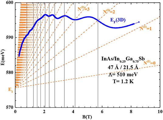
Figure 9. Calculated Landau levels of E1 as a function of the applied magnetic field in the investigated SL at 1.2 K. EF is the Fermi level energy.
In the Figure 9, when the magnetic field increases, the crossover between the calculated LL energy and the Fermi level gives the same minima (at B = 5.71 T, 4.13 T, 3.40 T, 2.73 T and 2.34 T), of the Shubnikov-de Haas effect (SDH) oscillations of the transverse magneto-resistance measured by Mitchel et al. [15].
The Figure 10 represents the computed 3D density of states (DOS) of the first conduction mini-band of the investigated SL by using the following expression [24]:
As can be seen in the figure the DOS is inversely proportional to the square root of total energy and the spacing between LL increases with the applied magnetic field.
A condition for the observation of the SDH effect is that the separation ℏωc (ωc = is the cyclotron pulsation) between LL must be superior to activation thermal energy kBT. So here the magnetic field must be B > kB T/ℏe = 0.9 T for T = 1.2 K and = 0.09 m0. When B < 0.9 T, the LLs disappear and E1 is a continuum. This condition of quantum limit agrees well with our calculated DOS (E1, B) in Figure 10.
We also calculated the transport scattering time τp = μH /e = 0.52 ps for Hall mobility μH = 1.02·104 cm2/Vs measured at 1.2 K by Mitchel et al. [18] and Haugan et al. [19] and our = 0.09 m0. This value of τp can be compared to the quantum relaxation time τq = 0.5 ps and τp = 2.34 ps measured in AlGaN/GaN two-dimensional electron gas [27].
Fuchs et al. [28] reported for the SL1 InAs(d1 = 34.8Å)/Ga0.8In0.2Sb(d2 = 29Å) with d1/d2 = 1.2, 8 μm ≤ λc ≤ 12 μm corresponding to 103 meV ≤ Eg ≤ 155 meV from electroluminescence for 10 K ≤ T ≤ 240 K. In the studied sample SL2 InAs(d1 = 47Å)/Ga0.75In0.25Sb(d2 = 21.5Å) with d1/d2 = 2.19, the insert of Figure 4 shows λc(T) with 7.46 ≤ λc(μm) ≤ 10.5 and 118 meV ≤ Eg ≤ 166 meV for the same investigated temperature range. In particular at low temperature, Eg(77K, SL1) = 150 meV from measured dynamical impedance increases to Eg(77K, SL2) = 157 meV in agreement with the fact that Eg increases when d1/d2 increases at a given temperature as seen in Figure 11. In the SL1, an electron effective mass of 0.03 m0 for transport perpendicular to the SL plane was used in the band-to-band tunneling model. This effective mass is in agreement with our 0.026 mo ≤ (kz) ≤ 0.028 mo for 1.2 K ≤ T ≤ 300 K near the center Γ of the first Brillion zone in Figure 6. All these transport parameters are in the same order of transport characteristics of the investigated SL.
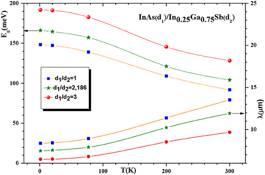
Figure 11. SLs Eg(Γ) and |λc(Γ)| as a function of temperature for various d1/d2 in InAs(d1)/Ga0.75In0.25Sb(d2) SL.
Using the envelope function formalism, we have investigated the electronic and optical properties of LWIR InAs(d1 = 2.18 d2)/In0.25Ga0.75Sb (d2 = 21.5 Å) type II SL. The dependencies of the band gap and the corresponding cut-off wavelength on layers' thicknesses and temperature were studied and interpreted. Our results show that a very smaller band gap can be achieved with reasonably thinner layers. The SC-SM transition was found to go to lower d1c and/or d2c when the temperature increases. Transport properties of this sample indicate a tridimensional conduction behavior. Whereas, the first valence subband HH1 shows 2D-like behavior. We interpreted the Shubnikov-de Haas effect and the density of states without and as a function of magnetic field. The condition of quantum limit agrees well with our calculations. In the intrinsic regime, our results agree well with experimental observations of W. C. Mitchel et al. These results are a guide for engineering infrared detectors.
All datasets generated for this study are included in the article/supplementary material.
NB: corresponding author doing the most of the article. AN: the supervisor is correcting the article. DB: help in the band gap calculation. AB, MB, SM, E-SE-S, and FC: help in calculation of masses effective and magnetotraport. All authors have contributed to this work and approved it for publication.
The authors declare that the research was conducted in the absence of any commercial or financial relationships that could be construed as a potential conflict of interest.
1. Smith DL, Mailhiot C. Theory of semiconductor superlattice electronic structure. Rev Mod Phys. (1990) 62:173. doi: 10.1103/RevModPhys.62.173
2. Boutramine A, Nafidi D, Barkissy E-S, El-Frikhe H, Charifi Elanique A, Chaib H. Electronic band structure and Shubnikov-de Haas effect in two-dimensional semimetallic InAs/GaSb nanostructure superlattice. Appl Phys A Mater Sci Process. (2016) 122:1. doi: 10.1007/s00339-015-9561-x
3. Grein CH, Lau WH, Harbert TL, Flatte ME. Modeling of very long infrared wavelength InAs/GaInSb strained layer superlattice detectors. Proc. SPIE, Materials for Infrared Detectors II Vol. 4795 (2002). doi: 10.1117/12.452265
4. Razeghi M, Minh Nguyen B. Advances in mid-infrared detection and imaging: a key issues review. Rep Prog Phys. (2014) 77:082401. doi: 10.1088/0034-4885/77/8/082401
5. Esaki L. Advances in semiconductor superlattices, quantum wells and heterostructures. J Phys Coll. (1984) 45:C5-3–C5-21. doi: 10.1051/jphyscol:1984501
6. Bastard G. Superlattice band structure in the envelope-function approximation. Phys Rev B. (1981) 24:5693.
7. Andlauer T, Vogl P. Full-band envelope-function approach for type-II broken-gap superlattices. Phys Rev. (2009) 80:035304. doi: 10.1103/PhysRevB.80.035304
8. Masur J-M, Rehm R, Schmitz J, Kirste L, Walther M. Infrared physics & technology. Science. (2013) 61:129–33. doi: 10.1016/j.infrared.2013.07.014
9. Barkissy D, Nafidi A, Boutramine A, Benchtaber N, Khalal A, El Gouti T. Electronic transport and band structures of GaAs/AlAs nanostructures superlattices for near-infrared detection. Appl Phys A. (2017) 123:61. doi: 10.1007/s00339-016-0629-z
10. Kane EO. Band structure of indium antimonide. J Phys Chem Solids. (1957) 1:249–61. doi: 10.1016/0022-3697(57)90013-6
11. Matossi F, Stern F. Temperature dependence of optical absorption in p-type indium arsenide. Phys Rev. (1958) 111:472. doi: 10.1103/PhysRev.111.472
12. Roth AP, Keeler WJ, Fortin E. Photovoltaic effect and temperature dependence of the energy gap in the In1–x GaxSb alloy system. Can Phys J. (1980) 58:560. doi: 10.1139/p80-079
13. Levinshtein M, Rumyantsev S, Shur M. (Eds.). Handbook series on semiconductor parameters. Vol. 1 Singapore: World Scientific Pub. Co. (1996). doi: 10.1142/2046-vol1
14. Gualtieri GJ, Schwartz GP, Nuzzo RG, Malik RJ, Walker JF. Determination of the (100) InAs/GaSb heterojunction valence band discontinuity by Xray photoemission core level spectroscopy. J Appl Phys. (1987) 61:5337. doi: 10.1063/1.338270
15. Mitchel WC, Elhamri S, Haugan HJ, Brown GJ, Mou S, Szmulowicz F. Shubnikov–de Haas Effect in InGaSb/InAs superlattices. J Appl Phys. (2017) 122:185106. doi: 10.1063/1.5010293
16. Kittel C. Introduction to Solid State Physics, 8th Edn. New York, NY: John Wiley & Sons. (2004). Available online at: https://www.wiley.com/en-us/9780471415268
17. Rogalski A. Infrared Detectors, 2nd Edn. Boca Raton, FL: CRC Press, Taylor and Francis Group. (2010). doi: 10.1201/b10319
18. Mitchel WC, Elhamri S, Haugan HJ, Brown GJ, Mou S, Szmulowicz F. Multicarrier transport in InGaSb/InAs superlattice structures. J Appl Phys. (2016) 120:175701. doi: 10.1063/1.4966136
19. Haugan HJ, Ullrich B, Elhamri S, Szmulowicz F, Brown GJ, Tung LC, et al. Magneto-optics of InAs/GaSb superlattices. J Appl Phys. (2010) 107:083112. doi: 10.1063/1.3391976
20. Szmulowicz F. Numerically stable secular equation for superlattices via transfer-matrix formalism and application to InAs/In0.23Ga0.77Sb and InAs/In0.3Ga0.7Sb/GaSb superlattices. Phys Rev B. (1998) 57:9081.
21. Szmulowicz F, Elhamri S, Haugan HJ, Brown GJ, Mitchel WC. Carrier mobility as a function of carrier density in type-II InAs/GaSb superlattices. J Appl Phys. (2009) 105:119901. doi: 10.1063/1.3137201
22. Szmulowicz F, Haugan HJ, Elhamri S, Brown GJ. Calculation of vertical and horizontal mobilities in InAs/GaSb superlattices. Phys Rev B. (2011) 84:155307. doi: 10.1103/PhysRevB.84.155307
23. Cho H-S. Density of states of quasi-two, -one, and -zero dimensional superlattices. J Vac Sci Technol B Microelectron Nano Struct. (1989) 7:1363. doi: 10.1116/1.584539
24. Seeger K. Semiconductor Physics: An introduction, 9th Edn. Berlin; Heidelberg: Springer. (2004). p. 296–303. doi: 10.1007/978-3-662-09855-4
25. Bastard G. Theoretical investigations of superlattice band structure in the envelope-function approximation. Phys Rev B. (1982) 25:7584. doi: 10.1103/PhysRevB.25.7584
26. Dresselhaus MS. Solid State Physics, Part III, Magnetic Properties of Solids (2018). p. 75–79. Available online at: http://web.mit.edu/6.732/www/6.732-pt3.pdf
27. Saxler A, Debray P, Perrin R, Elhamri S, Mitchel W, Elsass CR, et al. Electrical transport of an AlGaN/GaN two-dimensional electron gas. MRS Int J Nitride Semiconductor Res. (2000) 5:619–25. doi: 10.1557/S1092578300004841
Keywords: bands structure, quantum magneto transport, Shubnikov-de Haas effect, density of states, InAs/GaxIn1-xSb superlattice, infrared detection
Citation: Benchtaber N, Nafidi A, Barkissy D, Boutramine A, Benaadad M, Melkoud S, Es-Salhi E-S and Chibane F (2020) Correlation Between Bands Structure and Quantum Magneto Transport Properties in InAs/GaxIn1−xSb Type II Superlattice for Infrared Detection. Front. Phys. 8:52. doi: 10.3389/fphy.2020.00052
Received: 02 July 2019; Accepted: 20 February 2020;
Published: 18 March 2020.
Edited by:
Lorenzo Pavesi, University of Trento, ItalyReviewed by:
Philippe Christol, Université de Montpellier, FranceCopyright © 2020 Benchtaber, Nafidi, Barkissy, Boutramine, Benaadad, Melkoud, Es-Salhi and Chibane. This is an open-access article distributed under the terms of the Creative Commons Attribution License (CC BY). The use, distribution or reproduction in other forums is permitted, provided the original author(s) and the copyright owner(s) are credited and that the original publication in this journal is cited, in accordance with accepted academic practice. No use, distribution or reproduction is permitted which does not comply with these terms.
*Correspondence: Nassima Benchtaber, bmFzc2ltYWJlbmNAZ21haWwuY29t
Disclaimer: All claims expressed in this article are solely those of the authors and do not necessarily represent those of their affiliated organizations, or those of the publisher, the editors and the reviewers. Any product that may be evaluated in this article or claim that may be made by its manufacturer is not guaranteed or endorsed by the publisher.
Research integrity at Frontiers

Learn more about the work of our research integrity team to safeguard the quality of each article we publish.