
94% of researchers rate our articles as excellent or good
Learn more about the work of our research integrity team to safeguard the quality of each article we publish.
Find out more
REVIEW article
Front. Phys. , 15 November 2019
Sec. Optics and Photonics
Volume 7 - 2019 | https://doi.org/10.3389/fphy.2019.00190
 Xinping Zhang1*
 Jinghui Yang1,2
Plasmonic structures possess rich physics related to the sensitivity of plasmon resonance to the change in the environmental dielectric constant, the enhanced light scattering and optical extinction, and the local field enhancement enabled strong light-matter interactions, which have been applied in refractive-index sensors, optical feedback in various micro- or nano-cavity lasers, surface enhanced Raman scattering spectroscopy, and high-sensitivity molecular detection. However, ultrafast optical response is another important aspect of plasmons, which can be utilized to achieve switching of optical signals in different spectral bands. These optical switching designs are very important for applications in optical logic circuits and optical communication system. In this review, we summarize a series of reports on ultrafast plasmonic optical switches, where we focus our discussions on the structural and device designs, instead of on their physics. By categorizing the designs of optical switches into different groups by their featured performances, we intend to propose the development trend and the commonly interested mechanisms of such ultrafast optical switches. We hope this review will supply helpful concepts and technical approaches for further development and new applications of ultrafast optical switching devices.
Optical switching is indispensable in integrated optical logic circuits and optical communication systems [1–6]. High response speed, large modulation depth, and broadband acceptability or tunability are always expected for optical switching devices. Metallic nanostructures supply possibilities of ultrafast optical switching performance, where the fs-ps response time scale of surface plasmon resonance is a central mechanism [7–15]. Furthermore, incorporating plasmonic nanostructures into periodic photonic devices [16–20] enables amplification of the switching signal based on pure plasmonic spectral modulation, facilitating high-speed, high-efficiency, high signal-to-noise ratio, and low-threshold optical switching devices.
Localized surface plasmon resonance (LSPR) and surface plasmon polaritons (SPPs) are based on different forms of free electron oscillation in nanostructured metals under optical excitation. Such collective electronic oscillation has a lifetime shorter than 100 fs [5, 10, 11, 21–24], so that they supplied ideal mechanisms for ultrafast optical switching [25–52].
In this contribution, we review ultrafast plasmonic optical switching designs and devices by dividing them into a series of categories, which is based on the most important performances or intrinsic features in their constructions.
As generally accepted, plasmonic processes involve pure electronic process, electron-phonon interaction process, and pure phonon process, where the pure electronic process has coherent and in-coherent stages. For optical switching applications, we only make use of the electron-involved processes, i.e., the pure electronic process and the electron-phonon process. Thus, the speed of the switching is in a range from 100 fs to a few ps. However, depending on the pulse length and the pump-probe scheme, the switching speed may be much lowered. For instance, using pump and probe pulses longer than 100 fs, the switching signal is mostly a cross-correlation between the pump and probe pulses. Thus, the switching signal exhibits a nearly symmetric dynamic curve. In other words, the pump-probe detection cannot resolve the collective plasomic process. In such cases, the time duration of switching signal can be simply evaluated roughly by , where τp is the pulse length. Furthermore, as has been revealed that there exists an interference effect between the probe photons and the excited oscillation of plasmon electrons [7]. As shown in Figure 1A, the interference effect is a dynamics with in-phase and out-of-phase interaction between the probe pulse and the plasmon electron, resulting in alternative enhanced and reduced scattering or absorption of photons. As a result, oscillatory “fringes” can be observed in the switching signal dynamic curve. Such an effect nearly destroys the optical switching process by reducing largely the efficiency, expanding largely the switching signal or reducing the switching speed, and producing repeated on and off processes. As shown in Figure 1B, about two complete cycles of oscillation may be observed in the switching signal with a period of more than 200~300 fs. Apparently, the oscillation dynamics is actually a beat frequency oscillation between the pump and probe photons, verifying the interference nature of the interaction process.
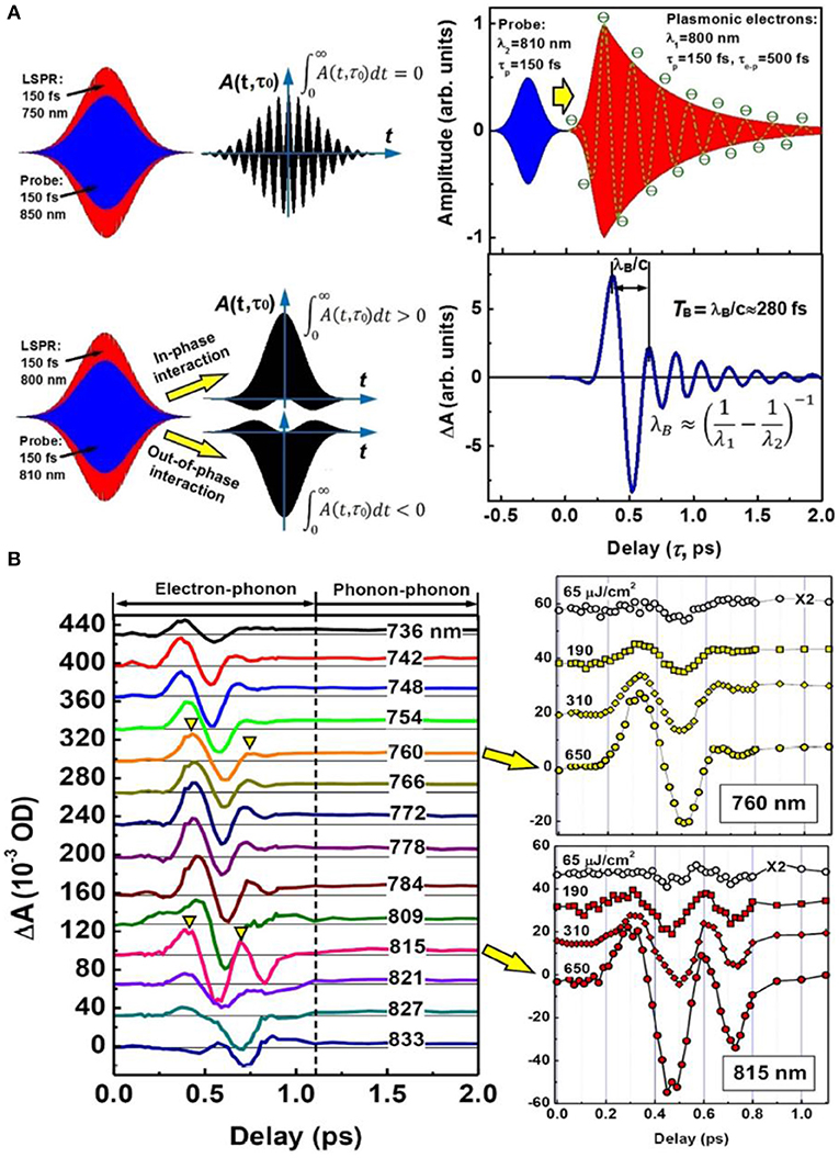
Figure 1. (A) Basic principles of beat oscillation in the interference-interaction between localized surface plasmon electrons and a probe photon. (B) Experimental observation of beat-oscillation processes in the interaction within 150-fs between a probe photon at 850 nm and the LSPR electrons oscillation at a wavelength of 750 nm. Reproduced with permission [7]. Copyright © 2016, the authors.
Thus, the interference effect should be always avoided in the design and operation of the optical switching device. It is understandable that the interference effect requires similar polarization of the pump and probe pulses. Therefore, it is recommended that the pump and the probe employ orthogonal polarizations. For instance, TM-pump and TE-probe scheme is recommended for the optical switch consisting of gold nanowire gratings.
In the design of ultrafast optical switching devices, the most important photophysical mechanisms that have been utilized include the electron-electron (e-e), electron-phonon (e-p), and phonon-phonon (p-p) scattering processes. All of these processes induced redshift of the plasmonic resonance spectrum and the optical switching processes could be achieved by the differential spectroscopic response. However, high switching speed in the scale of sub-100 fs can be achieved by the e-e process, although we mostly observe the e-p processes due to the long optical pulses. The p-p process is generally much slower and has smaller spectroscopic modulation depth as compared with the plasmonic electron-involved processes, which is observed as a long tail of the dynamics of optical switching signals. In metallic nanostructures, inter- or intra-band transitions in metal atoms can also be utilized to produce optical switching signals, which involve non-plasmonic processes. Considering that the optical switching processes originate mainly from spectral shift of the resonance signal, non-linear optical processes in the environmental medium can be utilized to achieve optical switching processes. Strong optical excitation induces transient change in the refractive index of the medium surrounding the plasmonic nanostructures, which results in the spectral shifts of plasmon resonance and consequently the switching of the probing light pulse. However, optical spectroscopic modulation by the changes in both the plasmonic modes and the environmental refractive index is generally very small. Incorporating the plasmonic nanostructures into photonic devices is an effective approach to amplify the optical switching signals. For instance, Fano coupling between the broad-band plasmons and the narrow-band photonic resonance modes has been utilized extensively for high-efficiency optical switches.
The simplest design is the device consisting of randomly distributed gold nanoparticles [26]. Optical excitation induced red shift of LSPR of the gold nanoparticles, so that difference spectroscopic response produced an optical switching signal. By depositing a further layer of continuous gold nanofilm, so that the isolated gold nanoparticles are connected together conductively, the spectroscopic response of the LSPR of the gold nanoparticles were much enhanced. As a result, the ultrafast spectroscopic response by femtosecond pump-probe detection showed large redshift and broadening of the resonance spectrum of the conductively connected gold nanoparticles (AuNPs) with respect to the isolated ones. The temporal and spectral dislocation between the edges of transition band is responsible for the much increased speed of the plasmonic optical switching effect.
A single Au/GeSbTe/Au nanosandwich structure was demonstrated for LSPR switching process [1]. The key mechanism is the hybridized palsmonic mode between an Au nanorod and the Au film, where a GeSbTe layer is inserted between these two plasmonic structures. The optical switching operation of the scattered light was achieved by the phase change between the amorphization and crystallization of GeSbTe when it is irradiated alternatively by picosecond laser pulses.
Plasmonic indium tine oxide (ITO) arrays (ITO-NRAs) have been utilized to achieve all optical switches in the infrared spectral band with high speed and high on/off ratios [2]. The switching operation is based on the optical excitation induced redshifts of LSPR in ITO nanorods. Significant plasmon frequency modulation and large transient bleaches and induced absorptions have been produced by strong optical excitation, which is based on the low electron density in ITO. Furthermore, the low electron heat capacity of ITO-NRAs enables sub-picosecond speed of the optical switching process.
Ultrafast optical dynamics has been revealed in nanostructured tungsten carbide (WC) [27]. Although this is not a direct demonstration of an optical switching device, the mechanisms based on LSPR in this conductive material is important for the design of all optical switches. It was discovered that strong optical excitation by femtosecond laser pulses induced transient modification on the energy-band structures in tungsten, which consequently resulted in the expansion and shift toward the Fermi level of the electronic d-band. This led to the lowering of the threshold photon energy for interband transitions, thus, producing enhanced transient absorption at a red-shifted spectrum, as shown in Figure 2. Furthermore, due to the enhanced density of states of the electronic band after transient modulation, electron density is also increased in the conduction band, which may enhance the LSPR effects. These mechanisms result in a rapid positive-to-negative transition in the transient absorption process, as shown in Figure 2D, which supplies a basis for ultrafast optical switching applications. The revealed mechanisms also apply to other metals and conductive materials.
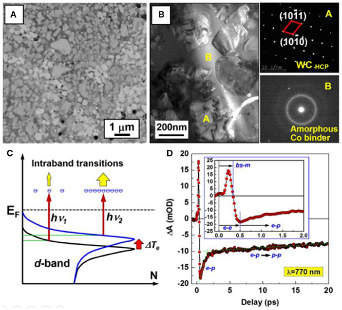
Figure 2. (A) SEM image of the surface of the WC coating. (B) TEM image (left panel) and SADPs of sites A and B (right panel). (C) Schematic illustration of modulation on the electronic band structures of W by strong optical excitation. (D) Dynamics of transient absorption (ΔA) measured at 770 nm on the surface of bulk tungsten. Inset: a closer look at the TA dynamics in the first 2 ps. Reproduced with permission [27]. Copyright © 2016, Optical Society of America.
Additionally, all-optical signal manipulation has been demonstrated by ultrafast photodoping and plasmon dynamics in fluorine–indium codoped cadmium oxide nanocrystals at optical communication wavelengths [3]. Ultrafast photodoping induced increase in carrier density and LSPR excitation led to a change in carrier effective mass. Large transmission modulation was achieved at modest pump powers in such a plasmonic material.
Surface plasmon polariton mode can be excited by sending a light beam onto a periodically modulated continuous metallic thin film. A wavevetor along the grating surface can be excited when the corresponding diffraction condition is satisfied. In a silver film deposited on an ITO grating, two SPP modes are excited at different spectra, which correspond to the propagation along the top and bottom interfaces of the silver film with air and ITO, respectively. Both modes exhibits ultrafast optical modulation dynamics under excitation by femtosecond laser pulses [28].
Figure 3A shows the design of the structures for the optical switching device and Figure 3B shows the geometry how the femtosecond pump-probe detection was carried out. Figures 3C,D present the TA spectra of the two SPP modes. The optical switching dynamics are shown in Figures 3E,F for the two modes at shorter and longer wavelengths, respectively. The speed of the optical switching was measured to be shorter than 300 fs for the longer-wavelength SPP.
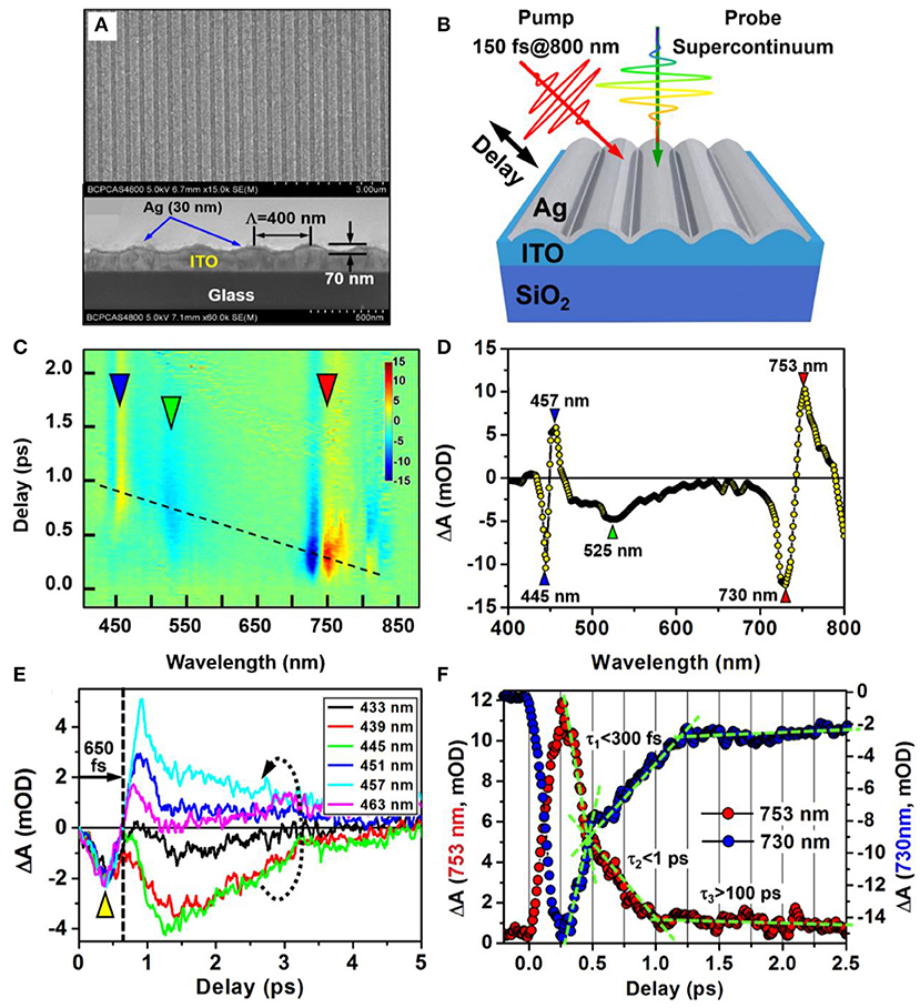
Figure 3. (A) SEM images of the Ag film deposited on an ITO grating. (B) Geometry of the pump probe measurements. (C) 3D plot of the TA spectra at different time delays between the pump and the probe. (D) TA spectrum at a delay of about 1 ps. (E) TA dynamics of the SPP modes at shorter wavelengths. (F) TA dynamics of the SPP mode at longer wavelengths. Reproduced with permission [28]. Copyright © 2019, Optical Society of America.
Fano coupling between a Fabry–Pérot cavity and a surface plasmon polariton (SPP) has been utilized to achieve optical switching and plasmonic modulation [8]. SPP mode was excited with a slit in a gold film and the Fabry-Pérot cavity was constructed by adding a second mirror with an adjustable separation from the bottom one, as shown in Figure 4A. Both the mechanical and electro-optical modulation have been utilized to switch the SPP emission. An ultrafast modulation with an efficiency of 30% has been achieved at a rate of ~ 0.6 THz for such a design.
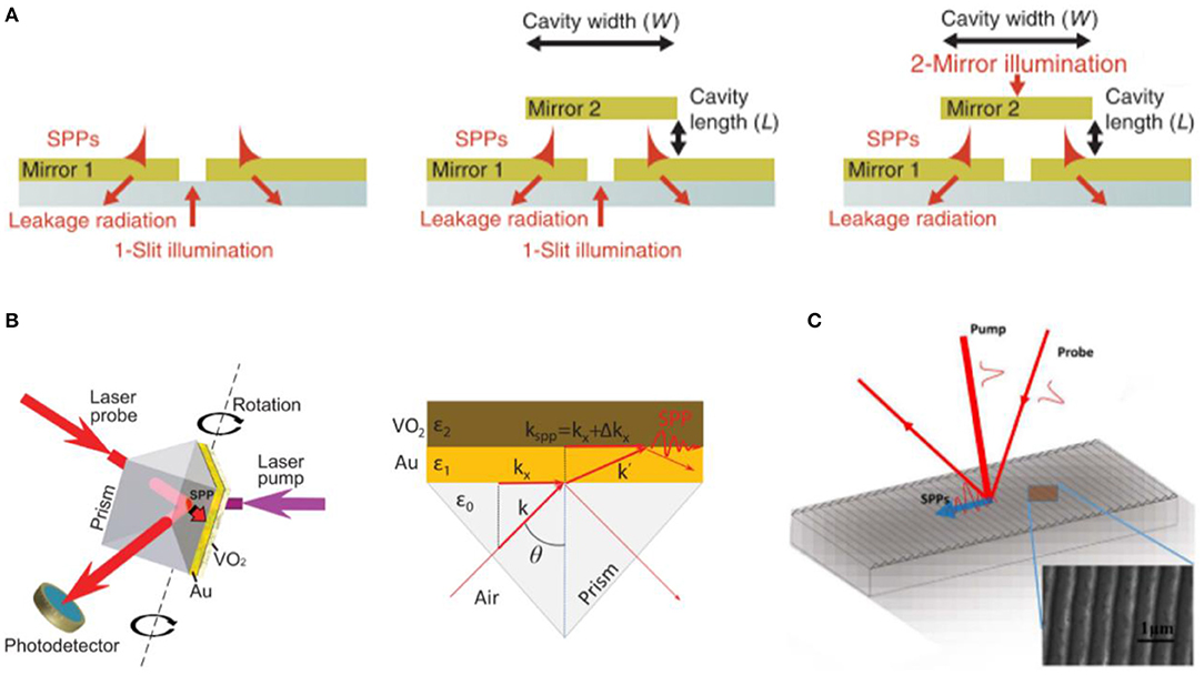
Figure 4. (A) Geometry of the switch composed of a cavity formed by two metal films with the bottom one containing a slit and acting as an SPP waveguide. Reproduced with permission [8]. Copyright © 2016, Spinger Nature. (B) Optical switch based on the excitation of SPPs at the VO2/Au interface. Reproduced with permission [9]. Copyright © 2018, Optical Society of America. (C) Ultrafast switching of the SPP in an aluminum-coated grating. Reproduced with permission [10]. Copyright © 2017, AIP Publishing.
On the basis of the SPP excitation in the gold film using the prism scheme, a layer of VO2 was produced on the top surface of gold, as shown in Figure 4B, so that optical switching was achieved by strong optical modulation on the SPP at the Au/VO2 interface, where the signal was detected in the reflection of the probe light beam [9]. The formation of the metallic phase of VO2 layer under strong optical excitation altered the field enhancement effects and the SPP propagation length at the VO2/Au interface, modulating the reflection spectrum around the SPP resonance. Such an optical manipulation of SPP resonance has a response speed of a picosecond timescale, supplying a design of optical switching device.
A further optical switching design based on direct excitation of SPPs was demonstrated by depositing aluminum onto a grating structure [10], as shown in Figure 4C. Propagation SPP mode was excited by the probe beam at a required angle of incidence, which is modulated by the pump pulse, producing sub-100-fs modulation in the reflection of the probe spectrum. Coherent non-linear interaction of the optical and SPP pulses was assigned as the responsible mechanisms.
Here we define hybrid plasmons by any structures that interfaced between different LSPs or SPPs. As defined in Figure 5A, hybrid plasmons are constructed between different structures (S1 ≠ S2) with different (M1 ≠ M2) or similar materials (M1 = M2) or the same structures (S1 = S2) with different materials (M1 ≠ M2). Normally metals are used as the plasmonic materials. Different structures may also be achieved by different shapes or different sizes of the same or different nanomaterials. The most important condition for the hybrid plasmons is the small separation distance between the nanostructures, which is generally required to be smaller than 20 nm for nanostructures or for plasmons resonant in the visible spectrum. Figure 5B shows some simple configurations of hybrid plasmonic structures. Such designs of hybrid plasmons largely extend the configurations of ultrafast optical switching devices. Figures 5C,D show some reported designs of hybrid plasmons of Au-Ag hetero-plasmonic dimers and Ag-Au-Ag bimetallic nanowires, respectively.
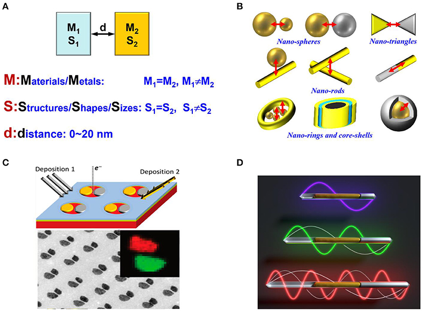
Figure 5. (A) Design of hybrid plasmons. (B) Some typical configurations of hybrid plasmonic schemes. (C) Au-Ag hetero-plasmonic dimers. Reproduced with permission [29]. Copyright © 2015, American Chemical Society. (D) Ag-Au-Ag bimetallic nanowires. Reproduced with permission [30]. Copyright © 2015, American Chemical Society.
The hybrid plasmonic structures have also been achieved by embedding silver nanoparticles into the hole space of a gold nanowire network [31]. Figure 6a shows the SEM image of such a structure and (Figure 6b) demonstrates the dark-field scattering image. According to the color difference in Figure 6b, the silver and gold nanostructures have different plasmon resonance performance. In particular, on the interface between gold and silver a third color can be observed, which can be taken as the response of the interfacial plasmon. Such structures are also potentially good candidates for optical switching devices.
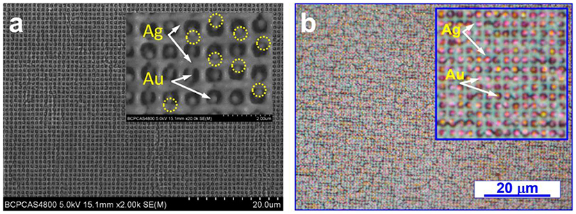
Figure 6. Hybrid plasmonic structures consisting of god nanowire network and embedded silver nanoparticles. (a) SEM images and (b) Dark-field optical microscope images of the fabricated structures. Reproduced with permission [31]. Copyright © 2018, John Wiley and Sons.
Single plasmonic nanoantenna embedded in ITO was demonstrated as a hybrid system for achieving a nano plasmonic optical switch with a picosecond response speed [32]. Large free-carrier non-linearity of ITO was enhanced by plasmon-induced hot-electron injection from the gold nanoantenna, which is the responsible mechanism for the optical switching effect, as shown in Figure 7A [32].
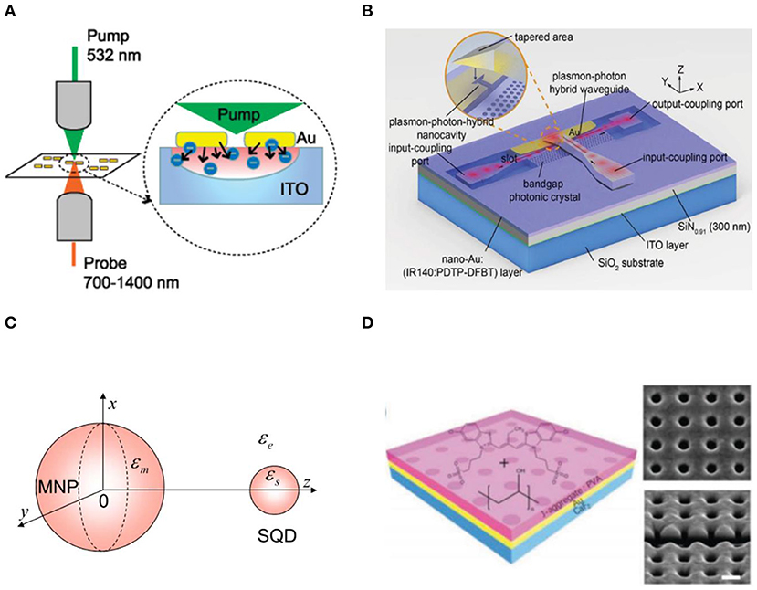
Figure 7. (A) Time-resolved reflectivity of single nanoantennas on high-conductivity ITO. Reproduced with permission [32]. Copyright © 2011, American Chemical Society. (B) On-Chip Optical Switch Based on Plasmon–Photon Hybrid Nanostructure-Coated Multicomponeonent Nanocomposite [4]. Copyright © 2016, American Chemical Society. (C) Schematic diagram of the hybrid system composed of a semiconductor quantum dot (SQD) and a metallic nanoparticle (MNP). Reproduced with permission [33]. Copyright © 2015, Optical Society of America. (D) Schematic diagram of a hybrid system composed of gold nanoholes array and J-aggregate molecules. Reproduced with permission [34]. Copyright © 2016, John Wiley and Sons.
An integrated photonic circuits design was demonstrated as an on-chip-triggered all-optical switch based on plasmon–photon hybrid nanostructures [4]. This multi-component nanocomposite design exhibits a low threshold pump intensity of 450 kW·cm−2, a fast response of 63 ps, and multiple operating wavelengths. Such a design is as shown in Figure 7B. An ultrafast optical switch is proposed in a quantum dot-metallic nanoparticle hybrid system [33], as depicted in Figure 7C. Interaction between a semiconductor quantum dot (SQD) and localized surface plasmons has been utilized to achieve ultrafast excitonic population inversion. A non-linearly chirped few-cycle pulse train excites enhanced plasmonic fields in a metallic nanoparticle and complete population inversion can be achieved in the SQD for small interparticle distance. The dynamics in population inversion exhibits a steplike transition between absorption and amplification, which may be utilized in optical switching effects.
Hybrid design of the plasmonic structures for optical switching devices have also been achieved by interactions between LSPs or SPPs and the J-aggregate excitons [11]. Transient optical Stark effects in such hybrid nanostructures have been utilized to achieve strong exciton-SPP coupling. Optical modulation dynamics in femtosecond time scales were demonstrated by transient spectroscopic response. Similar hybrid system has been reported in the coupling between J-Aggregate molecules and SPPs in subwavelength hole arrays, as illustrated in Figure 7D [34].
Nanostructured noble metals, including gold, and silver nanostructures [29–34], are the main group of materials that are utilized in ultrafast plasmonic optical switches. In an earlier work, waveguide gold nanowire grating has been demonstrated as a femtosecond optical switch, as shown in Figure 8A [19]. Fano-coupling between the waveguide resonance mode and localized surface plasmon in gold nanowires has been the responsible mechanism. A sub-200 fs speed and a 6% modulation depth have been achieved for such a device.
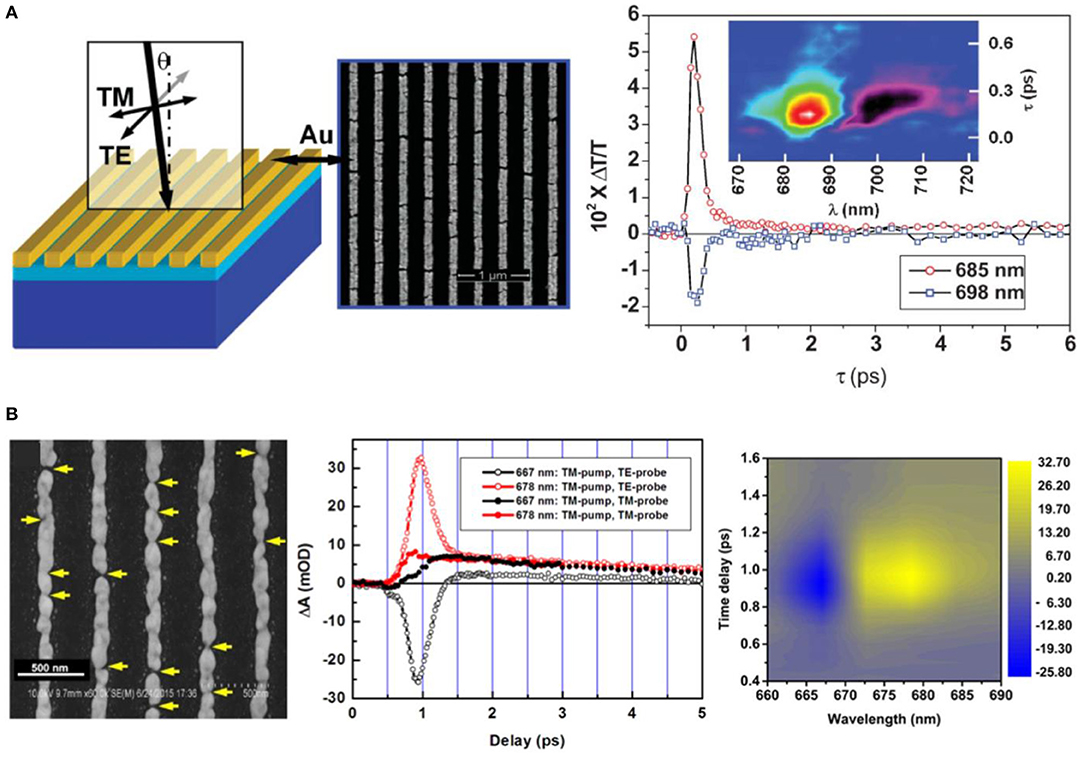
Figure 8. (A) Femtosecond optical switch using a waveguide gold nanowire grating. Reproduced with permission [19]. Copyright © 2008, John Wiley and Sons. (B) Femtosecond optical switch based on the optical heating of the interfacial palsmons induced at the gaps of discontinuous gold nanowires. Reproduced with permission [35]. Copyright 2017, the authors.
Also based on the waveguide gold nanowire grating structures, the gaps on the discontinuous gold nanowires have been utilized. Interfacial plasmons induced at these gaps may be modified due to optical heating by femtosecond laser pulses, where thermal expansion of the gold nanostructures changes the gap widths, as shown in Figure 8B. The “breathing” effect of the interfacial plasmon is responsible for the optical switching effect [35]. Furthermore, silver-coated gold nanorods [12] and gold nanoprism dimer [17] have been demonstrated as ultrafast optical switching structures.
Localized surface plasmons and SPPs in 2D materials with high charge-carrier mobility have also been utilized in ultrafast optical switches. Subwavelength-structured graphene exhibits plasmonic response in the mid infrared or terahertz spectral range. However, similar plasmon resonance effects as those for metallic nanostructures can also be observed and utilized in 2D materials like graphene, which attracts particular attention because the absence of an energy gap in graphene allows plasmon polaritons to be tuned continuously.
As shown in Figure 9, in subwavelength-scale graphene ribbons optical excitation induced red-shift of the plasmon resonance, which is a signature of hot charge carriers in the graphene and can be applied in optical switching devices [36]. Furthermore, small electronic specific heat in graphene enables fast control of plasmon resonance under transient heating of the charge carriers. This is important for applications in switching with high speed. As an alternative candidate to metallic materials for plasmons in the infrared, high-mobility graphene exhibits non-equilibrium photo-induced plasmonic performance. This is the basis for activating plasmons with femtosecond laser pulses and ultrafast pump-probe plasmonic control.
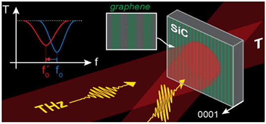
Figure 9. Optical switch using subwavelength-structured graphene surfaces. Reproduced with permission [36]. Copyright © 2019, American Chemical Society.
Different from graphene, another 2D material, the black phosphorous, is a van der Waals bonded semiconductor. Ultrashort near-infrared pulses enables high-contrast interband excitation of electron–hole pairs in black phosphorous, which is a promising material in surface polaritonics for ultrafast switching. A SiO2/black phosphorus/SiO2 heterostructure was designed to achieve an optical switching device in the infrared, which exhibits excellent switching contrast and switching speed [38].
Conductive metal oxides with high charge-carrier mobility also supply alternative routes to achieve plasmonic photonic devices [2]. Nanoparticles of doped indium tin oxide (ITO) nanoparticles have been incorporated into a photonic crystal structure, which exhibits photonic bandgap in the visible and plasmon resonance in the infrared [39]. Ultrafast optical switching based on tunable plasmon resonance through photodoping can be achieved in such a structure. The design and the microscopic characterization of the device are shown in Figure 10A [39] by the left panel and the optical switching dynamics by the right panel. Two-dimensional array of ITO nanorods has been used to achieve sub-picosecond optical switching process in the full visible spectral band, as shown in Figure 10B [40]. It is a demonstration that heavily doped wide-bandgap semiconductors can be used to realize all-optical control of light at a speed even faster than that of noble metals. Furthermore, the large aspect-ratio and low thermal conductivity of ITO enabled a slow optical modulation in the microsecond regime, which was associated with the slow lattice cooling.
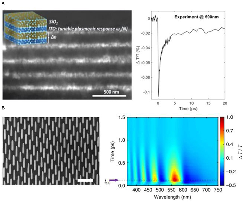
Figure 10. (A) Design of the plasmonic photonic device made of ITO nanoparticles and the optical switching performance. Reproduced with permission [39]. Copyright © 2018, Springer Nature. (B) Optical switching device consisting of an array of ITO nanorods and the transient absorption spectroscopic dynamics. Reproduced with permission [40]. Copyright © 2016, Springer Nature.
We define zero-dimensional design as a single plasmonic nanostructure, e.g., a sphere, a particle, a rod, a wire, and etc., which can be utilized to achieve optical switching effects. Wang et al. reported such a device using a single gold nanorod [41], as shown in Figure 11. Longitudinal (Lg) and transverse (Tr) surface plasmon resonance (SPR) modes were excited in the two orthogonal directions along and perpendicular to the axis of the gold nanorod, respectively. Two transient spectroscopic response signals were observed when the colloidal solution containing single gold nanorods was investigated by femtosecond pump-probe detection.
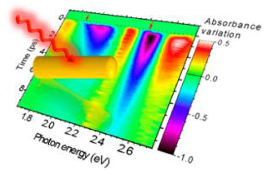
Figure 11. Dual resonance optical switching based on single gold nanorods. Reproduced with permission [41]. Copyright © 2015, American Chemical Society.
Two-dimensional (2D) design can be defined as structures with plasmon resonance or plasmonic hotspots located in the same plane that is generally parallel to the substrate. 2D periodical [10, 19, 28, 35] and non-periodical [26, 27] metallic nanostructures on planar substrates are most general designs of optical switching devices. A more typical design of a 2D periodic array of gold nanostructures is shown in Figure 12 [42]. Figure 12A shows the SEM image of the fabricated structures, which consist of hemisphere gold nanoshells connected by continuous gold film covering a 2D photoresist grating. Due to the geometry of the hemispheric nanoshells, the reflection spectrum is different in the space above and below the structures, which enables uni-directional performance of the plasmons and the optical switch, as shown in Figure 12B. A dipolar (DP) and hexapolar (HP) plasmon was observed when the reflection spectrum was measured in the space on the bottom of the structures. Thus, the optical switching performance can be characterized by femtosecond pump probe using the reflection mode on the bottom surface, as illustrated in Figure 12C. The two kinds of plasmonic resonance modes can also be observed in the transient absorption spectrum, as marked by HP at shorter wavelengths and DP at longer wavelengths in Figure 12D. Due to the different mechanisms for HP and DP modes, the optical switching by DP is much faster than that by HP, as shown in Figure 12E. For the DP mode, a switching speed of shorter than 300 fs and an amplitude of larger than 135 mOD (~27%) modulation on the reflection spectrum has been achieved.
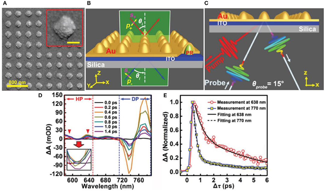
Figure 12. A 2D structure as plasmonic optical switch device consisting of an array of plasmonic hemisphere nanoshells. (A) SEM image of the plasmonic hemisphere nanoshells. (B) Design of the structures with directional spectroscopic response. (C) Reflection pump-probe scheme for the characterization of the optical switch. (D) TA spectra with a series of delay times, showing the spectral bands for hexapolar and dipolar resonance modes. (E) Normalized TA dynamics and the corresponding exponential fit curves at two typical wavelengths. Reproduced with permission [42]. Copyright © 2017, John Wiley and Sons.
Three-dimensional (3D) design can be defined as structures having multiple layers with each layer parallel or non-parallel to the substrate, where plasmon resonance or plasmonic hotspots are located in different layers or on the interface between different layers. Such a configuration was achieved in the two layer device consisting of cross-stacked gold nanowire gratings, which is shown in Figure 13 [43].
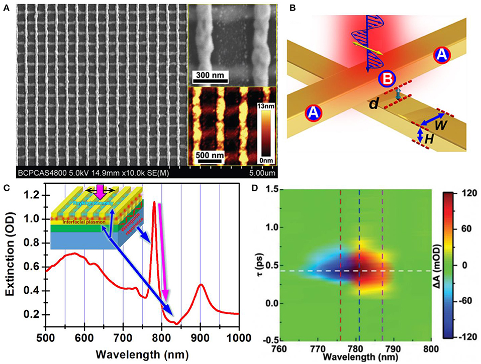
Figure 13. (A) A 3D structure consisting of cross-stacked gold nanowire gratings. (B) Interfacial plasmon excited between two cross-stacked gold nanowires. (C) Interaction between multiple resonance modes induced narrow-band spectroscopic response. (D) Optical switching performance characterized by transient absorption spectroscopic response. Reproduced with permission [43]. Copyright © 2015, the authors.
Figure 13A shows the practically fabricated structures by the SEM and AFM images. The central mechanism for such a design is the interfacial plasmon at the crossing point between the two perpendicularly arranged gold nanowires with a separation of d< 20 nm, as shown in Figure 13B. Meanwhile, there are multiple further resonance modes: waveguide resonance mode in the gold nanowire grating on the ITO waveguide, Rayleigh anomaly in the gold nanowire grating on the top layer, and Fano coupling between Rayleigh anomaly and the interfacial plasmon. Interaction between all of above resonance modes produces a sharp spectrum in the transmissive optical extinction, as shown in Figure 13C, which favors high-efficiency optical switching. The femtosecond transient absorption spectroscopy verifies an excellent optical switching device with a speed faster than 280 fs and an on/off modulation depth of about 22.4%, as shown in Figure 13D.
Most of the reported ultrafast plasmonic optical switches have been working in the visible spectral range [39, 40, 44–46]. This is because plasmonic resonance of most nanostructured noble metals has spectroscopic response in the visible band. Such structures are more easily designed and fabricated, as compared with those in the infrared or at even longer wavelengths. Therefore, there is a large overlap between the plasmonic optical switching devices operating in the visible spectral range with those categorized into material designs [39, 46], structural designs [40, 44], and plasmonic mode designs [45] in above sections. Thus, we do not need to make more discussions on this category of devices.
Shifting the plasmonic resonance spectrum to the infrared may be realized in the following ways: (1) Using large-sized metallic nano- or even micro-structures, where these structures generally need to have small aspect ratios. (2) Embedding the plasmonic nanostructures in a medium with large dielectric constants. (3) Constructing plasmonic nano- or micro-structures using conductive materials with relative lower charge mobility, e.g., using nanostructures of metal oxides or 2D materials, other than metals. (4) Combining metallic structures with dielectric or semiconducting materials to achieve hybrid structures, e.g., metal-isolator-metal (MIM) structures.
An optical switching device with a sub-ps speed has been achieved in colloidal nanocrystals of epsilon-near-zero materials working in the near- to mid-infrared with a spectral range from 1.5 to 3.0 μm [47]. Such solution-processed nanocrystals exhibit interestingly different spectroscopic performance under intra-and inter-band excitation. Intraband excitation induces red shift of the plasmon features due to the low electron heat capacities and conduction band non-parabolicity of the oxide, however, interband excitation pulls the plasmon resonance to the blue due to the transient increase in the carrier density. These performances enable promising applications of such materials in ultrafast all-optical switching. Also using solution-processed oxide nanoparticles, all-optical switching devices have been reported in the mid-infrared [48]. Broadly tunable mid-infrared (MIR) plasmons have been exploited in solution-processed and degenerately doped oxide nanoparticles. Such a switch shows a sub-ps speed in the mid-infrared spectral band extending from 3.0 to 5.0 μm.
An ultrafast plasmonic optical switch was proposed in the near infrared using the combination of plasmonic structures with Kerr materials [5]. The device was supposed to be constructed using a Kerr non-linear ring resonator on a metal–insulator–metal (MIM) nanoplasmonic waveguide. Simulations show an optical bistability and a switching process with a femtosecond-scale feedback time. Another optical switch using Au nanostripes has been demonstrated to work in the near infrared [49].
Recently, plasmonic optical control in the terahertz region has been extensively reported. This is based on the rapid development and the extended applications of THz techniques. However, in such optical switching schemes, pumping the plasmonic materials or structures using ultrashort laser pulses in the visible or infrared have been the mostly employed designs.
An optical switching of THz pulses has been achieved using an array of Bi2Se3 micro ribbons, which is a topographic insulator [50]. A modulation depth as large as 2,400% has been achieved at 1.5 THz, which was measured at an optical fluence as low as 45 mJ/cm2. A THz plasmonic switching device was demonstrated using a 2D micro-nanostructured metal film with hole arrays [51] The construction of the device is based on a 2D aluminum hole array above a layer of silicon, where the device was fabricated on a sapphire substrate. Excitation of the silicon layer using different colors of light enabled different ultrafast switching of the THz waves. The color-sensitive performance extends the application of such a THz modulation device.
An artificial material made of split-ring resonators have been demonstrated as an optical pumped THz switch [52]. The blue-shift and band broadening of the transmission spectrum under optical excitation is responsible for the switching process. The change in the refractive index and conductivity of the semiconductor substrate induced by photoexcitation is the basic mechanism for the blue-shift effect.
Furthermore, Au/CdTe plasmonic crystals have been constructed by fabrication a plasmonic grating of Au nanostripes on a substrate of telluride-based II-VI semiconductors. Femtosecond optical pulse excitation induced segregation of Te and produced a tellurium layer at the interface between Au and the substrate. Surface plasmon polaritons under optical excitation was responsible for the formation of the tellurium layer. The lattice vibrations caused a shift of the phonon frequency in the nm-thick segregated tellurium layer. Thus, in the femtosecond pump-probe measurement a THz modulation dynamics was observed. It needs to be noted that this is in fact not a switching of THz waves, instead, it is a modulator of optical pulses with a frequency of THz. This can be taken as another aspect of the optical switching performance [49].
Ultrafast optical switching devices based on plasmonic nano- or micro-structures possess multifold advantageous features, including high speed due to the fast collective electron scattering process, high stability and high damage threshold based on metallic nanostructures, and high signal contrast due to the generally narrow-band resonance modes through interaction between plasmonic and photonic processes. However, femtosecond optical pulse excitation implies high pump fluence, so that it is always important to reduce the excitation threshold for the optical switches. Ultrashort laser pulses produced by laser amplifiers with a pulse energy fluence in the scale of 100 μJ-mJ/cm2 have been employed in most of the reported devices. For more practical applications, ultrafast optical switching using femtosecond laser pulses with an energy in nJ or sub-μJ is more desired, where mode-locked laser oscillators, instead of amplifiers, are strong enough to supply the excitation.
Miniaturization of the optical switching devices is another important aspect of further development. Plasmonic nanostructures with multifold functions or hybridization of various nanostructures or nanomaterials should be considered in the designs and constructions. Such considerations are important for on-chip optical circuits or integration of the optical logic device onto large-scale optical calculation systems. Integration of the optical switch devices onto end facets of optical fibers is also an important development route for the application in optical communication systems.
Optical switching devices in the infrared and the THz spectral bands are more fascinating and becoming more interested for applications. In these designs, due to the low intensity of the THz waves, ultrashort laser pulses in the visible or infrared are usually used as the pump. However, the detection and manipulation of the THz waves are still a challenge for such applications. Therefore, the corresponding development is dependent more on the progress in the THz generation and detection techniques.
We review a variety of ultrafast optical switching devices based on plasmonic structures. We summarized a series of designs by categories of different plasmons, different conductive materials, different dimensions of the structures, and different working spectral bands. These structural and device designs supply ultrafast optical signal control techniques for different applications. Thus, extensive strategies are potentially applicable for incorporating plasmonic nanostructures into optical logic circuits and optical communication system. This review also intends to excite more innovative investigations on new plasmonic materials and structures in the design of ultrafast optical switching techniques.
XZ designed this work, did the analysis of the research works, and wrote the paper. JY helped with the literature collection.
The authors declare that the research was conducted in the absence of any commercial or financial relationships that could be construed as a potential conflict of interest.
The authors acknowledge the National Natural Science Foundation of China (NSFC) (61735002, 11574015, 11434016) and the 973 Program (2013CB922404) for the support.
1. Hira T, Homma T, Uchiyama T, Kuwamura K, Kihara Y, Saiki T. All-optical switching of localized surface plasmon resonance in single gold nanosandwich using GeSbTe film as an active medium. Appl Phys Lett. (2015) 106:031105–5. doi: 10.1063/1.4906037
2. Guo PJ, Schaller RD, Ketterson JB, Chang RPH. Ultrafast switching of tunable infrared plasmons in indium tin oxide nanorod arrays with large absolute amplitude. Nat Photon. (2016) 10:267–74. doi: 10.1038/nphoton.2016.14
3. Kriegel I, Urso C, Viola D, De Trizio L, Scotognella F, Cerullo G, et al. Ultrafast photodoping and plasmon dynamics in fluorine–indium codoped cadmium oxide nanocrystals for all-optical signal manipulation at optical communication wavelengths. J Phys Chem Lett. (2016) 7:3873–81. doi: 10.1021/acs.jpclett.6b01904
4. Chai Z, Zhu Y, Hu XY, Yang X, Gong ZB, Wang FF, et al. On-chip optical switch based on plasmon–photon hybrid nanostructure-coated multicomponeonent nanocomposite. Adv Opt Mater. (2016) 4:1159–66. doi: 10.1002/adom.201600271
5. Nurmohammadi T, Abbasian K, Yadipour R. Ultra-fast all-optical plasmonic switching in near infra-red spectrum using a Kerr nonlinear ring resonator. Opt Commun. (2018) 410:142–7. doi: 10.1016/j.optcom.2017.09.082
6. Baig SA, Boland JL, Damry DA, Tan HH, Jagadish C, Joyce HJ, et al. An ultrafast switchable terahertz polarization modulator based on III–V semiconductor nanowires. Nano Lett. (2017) 17:2603–10. doi: 10.1021/acs.nanolett.7b00401
7. Zhang XP, He JF, Wang YM, Liu FF. Terahertz beat oscillation of plasmonic electrons interacting with femtosecond light pulses. Sci Rep. (2016) 6:18902–8. doi: 10.1038/srep18902
8. McPolin CP, Olivier N, Bouillard J-S, O'Connor D, Krasavin AV, Dickson W, et al. Universal switching of plasmonic signals using optical resonator modes. Light Sci Appl. (2017) 6:e16237–8. doi: 10.1038/lsa.2016.237
9. Kumar N, Rúa A, Aldama J, Echeverria K, Fernández FE, Lysenko S. Photoinduced surface plasmon switching at VO2/Au interface. Opt Exp. (2018) 26:11068–77. doi: 10.1364/OE.26.013773
10. Wang KD, Chen L, Zhang HJ, Chen J. Controlling surface plasmon polaritons at femtosecond timescales on an aluminum-coated grating. Appl Phys Lett. (2017) 110:021105–4. doi: 10.1063/1.4973860
11. Vasa P, Wang W, Pomraenke R, Maiuri M, Manzoni C, Cerullo G, et al. Optical Stark effects in J-aggregate–metal hybrid nanostructures exhibiting a strong exciton–surface-plasmon-polariton interaction. Phys Rev Lett. (2015) 114:036802–6. doi: 10.1103/PhysRevLett.114.036802
12. Dai HW, Zhang LM, Wang ZW, Wang X, Zhang JP, Gong HM, et al. Linear and nonlinear optical properties of silver-coated gold nanorods. J Phys Chem C. (2017) 121:12358–64. doi: 10.1021/acs.jpcc.7b00295
13. Wang H, Wang HY, Toma A, Yano TA, Chen QD, Xu HL, et al. Dynamics of strong coupling between CdSe quantum dots and surface plasmon polaritons in subwavelength hole array. J Phys Chem Lett. (2016) 7:4648–54. doi: 10.1021/acs.jpclett.6b02059
14. Kim J, Carnemolla EG, DeVault C, Shaltout AM, Faccio D, Shalaev VM, et al. Dynamic control of nanocavities with tunable metal oxides. Nano Lett. (2018) 18:740–6. doi: 10.1021/acs.nanolett.7b03919
15. Della Valle G, Polli D, Biagioni P, Martella C, Giordano MC, Finazzi M, et al. Self-organized plasmonic metasurfaces for all-optical modulation. Phys Rev B. (2015) 91:235440–10. doi: 10.1103/PhysRevB.91.235440
16. Sim S, Jang H, Koirala N, Brahlek M, Moon J, Sung JH, et al. Ultra-high modulation depth exceeding 2,400% in optically controlled topological surface plasmons. Nat Commun. (2015) 6:9814–7. doi: 10.1038/ncomms9814
17. Lu CC, Hu XY, Shi KB, Hu Q, Zhu R, Yang H, Gong QH. An actively ultrafast tunable giant slow-light effect in ultrathin nonlinear metasurfaces. Light Sci Appl. (2015) 4:e302–9. doi: 10.1038/lsa.2015.75
18. Thomas A, Savaliya P, Kumar K, Ninawe A, Dhawan A. Au nanowire-VO2 spacer-Au film based optical switches. J Opt Soc Am B. (2018) 35:1687–97. doi: 10.1364/JOSAB.35.001687
19. Zhang XP, Sun BQ, Hodgkiss JM, Friend RM. Tunable ultrafast optical switching via waveguided gold nanowires. Adv Mater. (2008) 20:4455–9. doi: 10.1002/adma.200801162
20. Sharma Y, Tiruveedhula VA, Muth JF, Dhawan A. VO2 based waveguide-mode plasmonic nanogratings for optical switching. Opt Express. (2015) 23:5822–49. doi: 10.1364/OE.23.005822
21. Link S, El-Sayed MA. Size and temperature dependence of the plasmon absorption of colloidal gold nanoparticles. J Phys Chem B. (1999) 103:4212–7. doi: 10.1021/jp984796o
22. Klein-Wiele JH, Simon P, Rubahn HG. Size-dependent plasmon lifetimes and electron-phonon coupling time constants for surface bound Na clusters. Phys Rev Lett. (1998) 80:45–8. doi: 10.1103/PhysRevLett.80.45
23. Ropers C, Park DJ, Stibenz G, Steinmeyer G, Kim J, Kim DS, et al. Femtosecond light transmission and subradiant damping in plasmonic crystals. Phys Rev Lett. (2005) 94:113901–4. doi: 10.1103/PhysRevLett.94.113901
24. Kim DS, Hohng SC, Malyarchuk V, Yoon YC, Ahn YH, Yee KJ, et al. Microscopic origin of surface-plasmon radiation in plasmonic band-gap nanostructures. Phys Rev Lett. (2003) 91:143901–4. doi: 10.1103/PhysRevLett.91.143901
25. Sun X, Chen X, Yan M, Qiu M, Thylén L, Wosinski L. All-optical switching using a hybrid plasmonic donut resonator with photothermal absorber. IEEE Photonic Tech Lett. (2016) 28:1609–12. doi: 10.1109/LPT.2016.2558478
26. Cun P, Wang M, Huang CY, Huang P, He XK, Zhang XP. Conductive connection induced speed-up of localized-surface-plasmon dynamics. J Opt. (2018) 20:014011–6. doi: 10.1088/2040-8986/aa9f47
27. Zhang XP, Wang HB, Wang M, Lin YH, Song XY. Ultrafast particle-plasmon enhancement by energy-band modification in nanostructured tungsten carbide. Opt Express. (2016) 24:22730–40. doi: 10.1364/OE.24.022730
28. Zhang J, Zhang XP. Ultrafast plasmon polaritons doubly resonant on a single silver nanoshell. Opt Express. (2019) 27:17061–8. doi: 10.1364/OE.27.017061
29. Zhang ML, Large N, Koh AL, Cao Y, Manjavacas A, Sinclair R, et al. High-density 2D homo- and hetero- plasmonic dimers with universal sub-10-nm gaps. ACS Nano. (2015) 9:9331–9. doi: 10.1021/acsnano.5b03090
30. Mayer M, Scarabelli L, March K, Altantzis T, Tebbe M, Kociak M, et al. Controlled living nanowire growth: precise control over the morphology and optical properties of AgAuAg bimetallic nanowires. Nano Lett. (2015) 15:5427–37. doi: 10.1021/acs.nanolett.5b01833
31. Zhang J, Zhang XP. Bimetallic network with hetero-interfacial plasmons. Adv Mater Interfaces. (2018) 5:1800580–7. doi: 10.1002/admi.201800580
32. Abb M, Albella P, Aizpurua J, Muskens OL. All-optical control of a single plasmonic nanoantenna-ITO hybrid. Nano Lett. (2011) 11:2457–63. doi: 10.1021/nl200901w
33. Yang WQ, Chen AX, Huang ZW, Lee RK. Ultrafast optical switching in quantum dot-metallic nanoparticle hybrid systems. Opt Express. (2015) 23:13032–40. doi: 10.1364/OE.23.013032
34. Wang H, Wang HY, Bozzola A, Toma A, Panaro S, Raja W, et al. Dynamics of strong coupling between J-Aggregates and surface plasmon polaritons in subwavelength hole arrays. Adv Funct Mater. (2016) 26:6198–205. doi: 10.1002/adfm.201601452
35. Wang YM, Zhang XP, Fang XH. Ultrafast optical heating induced polarization-dependent optical switching in gold nanowires. Appl Sci. (2017) 7:46–8. doi: 10.3390/app7010046
36. Jadidi MM, Daniels KM, Myers-Ward RL, Gaskill DK, König-Otto JC, Winnerl S, et al. Optical control of plasmonic hot carriers in graphene. ACS Photon. (2019) 6:302–7. doi: 10.1021/acsphotonics.8b01499
37. Ni GX, Wang L, Goldflam MD, Wagner M, Fei Z, McLeod AS, et al. Ultrafast optical switching of infrared plasmon polaritons in high-mobility grapheme. Nat Photon. (2016) 10:244–8. doi: 10.1038/nphoton.2016.45
38. Huber MA, Mooshammer F, Plankl M, Viti L, Sandner F, Kastner LZ, et al. Femtosecond photo-switching of interface polaritons in black phosphorus heterostructures. Nat Nanotechnol. (2017) 12: 207–12. doi: 10.1038/nnano.2016.261
39. Paternò GM, Iseppon C, D'Altri A, Fasanotti C, Merati G, Randi M, et al. Solution processable and optically switchable 1D photonic structures. Sci Rep. (2018) 8:3517–8. doi: 10.1038/s41598-018-21824-w
40. Guo PJ, Schaller RD, Ocola LE, Diroll BT, Ketterson JB, Chang RP. Large optical nonlinearity of ITO nanorods for sub-picosecond all-optical modulation of the full-visible spectrum. Nat Commun. (2016) 7:12892–10. doi: 10.1038/ncomms12892
41. Wang XL, Guillet Y, Selvakannan PR, Remita H, Palpant B. Broadband spectral signature of the ultrafast transient optical response of gold nanorods. J Phys Chem C. (2015) 119:7416–27. doi: 10.1021/acs.jpcc.5b00131
42. Lin YH, Zhang XP. Ultrafast multipolar plasmon for unidirectional optical switching in a hemisphere-nanoshell array. Adv Opt Mater. (2017) 5:1601088–8. doi: 10.1002/adom.201601088
43. Lin YH, Zhang XP, Fang XH Liang SY. A cross-stacked plasmonic nanowire network for high-contrast femtosecond optical switching. Nanoscale. (2015) 8: 1421–9. doi: 10.1039/C5NR06464C
44. Grinblat G, Berté R, Nielsen MP, Li Y, Oulton RF, Maier SA. Sub-20 fs all-optical switching in a single Au-clad Si nanodisk. Nano Lett. (2018) 18:7896–900. doi: 10.1021/acs.nanolett.8b03770
45. Taghinejad M, Taghinejad H, Xu ZH, Lee KT, Rodrigues SP, Yan JH, et al. Ultrafast control of phase and polarization of light expedited by hot-electron transfer. Nano Lett. (2018) 18:5544–51. doi: 10.1021/acs.nanolett.8b01946
46. Guo PJ, Weimer MS, Emery JD, Diroll BT, Chen XQ, Hock AS, et al. Conformal coating of a phase change material on ordered plasmonic nanorod arrays for broadband all-optical switching. ACS Nano. (2017) 11:693–701. doi: 10.1021/acsnano.6b07042
47. Diroll BT, Guo PJ, Chang RPH, Schaller RD. Large transient optical modulation of epsilonnear-zero colloidal nanocrystals. ACS Nano. (2016) 10:10099–105. doi: 10.1021/acsnano.6b05116
48. Guo QB, Qin ZP, Wang Z, Weng YX, Liu XF, Xie GQ, et al. Broadly tunable plasmons in doped oxide nanoparticles for ultrafast and broadband mid-Infrared all-optical switching. ACS Nano. (2018) 12:12770–7. doi: 10.1021/acsnano.8b07866
49. Kreilkamp LE, Akimov IA, Belotelov VI, Glavin BA, Litvin LV, Rudzinski A, et al. Terahertz dynamics of lattice vibrations in Au/CdTe plasmonic crystals: Photoinduced segregation of Te and enhancement of optical response. Phys Rev B. (2016) 93:125404–10. doi: 10.1103/PhysRevB.93.125404
50. Valdés Aguilar R, Qi J, Brahlek M, Bansal N, Azad A, Bowlan J, et al. Time-resolved terahertz dynamics in thin films of the topological insulator Bi2Se3. Appl Phys Lett. (2015) 106:011901–5. doi: 10.1063/1.4905438
51. Kumar A, Srivastava YK, Manjappa M, Singh R. Color-sensitive ultrafast optical modulation and switching of terahertz plasmonic devices. Adv Opt Mater. (2018) 6:1800030–6. doi: 10.1002/adom.201800030
Keywords: ultrafast optical switching, plasmonic nanostructures, plasmonic device, surface plasmon polariton, hybrid plasmons, noble metals, metal oxides, 2D materials
Citation: Zhang X and Yang J (2019) Ultrafast Plasmonic Optical Switching Structures and Devices. Front. Phys. 7:190. doi: 10.3389/fphy.2019.00190
Received: 31 August 2019; Accepted: 30 October 2019;
Published: 15 November 2019.
Edited by:
Yanpeng Zhang, Xi'an Jiaotong University, ChinaCopyright © 2019 Zhang and Yang. This is an open-access article distributed under the terms of the Creative Commons Attribution License (CC BY). The use, distribution or reproduction in other forums is permitted, provided the original author(s) and the copyright owner(s) are credited and that the original publication in this journal is cited, in accordance with accepted academic practice. No use, distribution or reproduction is permitted which does not comply with these terms.
*Correspondence: Xinping Zhang, emhhbmd4aW5waW5nQGJqdXQuZWR1LmNu
Disclaimer: All claims expressed in this article are solely those of the authors and do not necessarily represent those of their affiliated organizations, or those of the publisher, the editors and the reviewers. Any product that may be evaluated in this article or claim that may be made by its manufacturer is not guaranteed or endorsed by the publisher.
Research integrity at Frontiers
Learn more about the work of our research integrity team to safeguard the quality of each article we publish.