- 1Department of Condensed Matter Physics and Material Sciences, Tata Institute of Fundamental Research, Mumbai, India
- 2Department of Electrical Engineering, Indian Institute of Technology, Mumbai, India
We present 2-, 3-, and 6-way optical demultiplexer and optical filters based on coupled waveguide and photonic crystal cavities. Demultiplexers with 3 nm channel separation and optical splitters with different transmission efficiencies are presented. The structures designed on GaAs wafers having the smallest footprint of 78 μm2, are suitable for integrating all-optical devices for planar integrated circuits.
Introduction
Planar architectures offer compact in-plane circuits that can help miniaturize the photonic devices. While for classical communication, devices with fine channel separation are interesting [1–4], these can also have applications in quantum information processing when few photon level responses are achieved [5–10]. Photonic crystal (PC) based planar designs offer integrated chip architectures in which by employing non-linear optical materials, one can achieve ultrafast active control and novel functionalities [11]. Feasibility of PC based planar circuits for quantum information is reported on InAs/GaAs quantum dot (QD) spin to photon conversion to read out the electron spin state in a QD by measuring the complete polarization of emitted photon [10, 12]. A coupled cavity architecture suitable for multi-qubit operations and studying non-local interactions between QDs was also reported [13]. Thus, PC architectures are interesting for both classical and quantum information processing.
The performance of PC based demultiplexers/splitters depends on the number of output channels, crosstalk, channel separation, transmission efficiency, footprint, and ease of fabrication. A number of proposals have been put forward to improve these characteristics. Barnier et al. [14] have provided a design based on super-prism with a channel spacing of 25 nm and crosstalk level of about −16 db. Momeni et al. reported a channel spacing of 8 nm with the highest crosstalk level of −6.5 db by combining super prism effect with negative diffraction and refraction [15]. Cheng et al. have proposed a five-channel demultiplexer based on silicon rods of periodic lattice with a channel spacing of 8 nm [16]. Rostami et al. [17, 18] have proposed a design for 4-channel demultiplexer by combining a T-branch waveguide with four resonant cavities with a channel spacing of 0.8 nm, crosstalk level better than −18.8 dB and with a footprint of 536 μm2. A cascaded three PC ring resonator-based channel drop filters with different refractive indices to realize a four-channel demultiplexer with a channel spacing of about 6.1 nm with an average transmission efficiency of 95% with crosstalk better than −24.44 dB was reported in a structure with footprint of 294.25 μm2 [19]. Alipour-Banaei et al. [20] proposed a resonant defect structure for designing eight-channel demultiplexer with the channel spacing of about 1 nm, minimum transmission efficiency and the largest crosstalk of 40% and −8 dB, respectively, and footprint of 498 μm2. Mehdizadeh and Soroosh presented an eight-channel demultiplexer design based on defective resonant cavities in a square lattice with rods-in-air approach [21]. The transmission efficiency was obtained in the 94–99% range with crosstalk better than −11.2 dB and footprint of 495 μm2. PC waveguides with phase mismatch introduced by shifting the waveguide wall airholes with respect to the others were demonstrated [22]. In these, the phase mismatch leads to mode splitting which can be employed to achieve fine channel separation. Efficient PC cavity-waveguide couplers with up to 90% coupling efficiency were shown earlier [23].
In this article, we propose coupled cavity-waveguide architecture to demonstrate splitters and demultiplexers with the smallest footprint. Multiple waveguides, each optimized for different wavelength and, coupled to individual cavities are designed to demonstrate 2-, 3-, and 6-way splitters and DEMUX applications. While the waveguides couple radiation from the central source to different arms, each cavity is useful for out of plane coupling. Schematic of these structures are shown in Figure 1. The air in dielectric approach is considered to achieve a fairly high transmission efficiency, crosstalk better than −2.2db, and footprint of 78 μm2 which is much smaller than those proposed so far. The novelty of the design lies in using the same structure with different parameters to be used as optical splitter or optical demultiplexer.
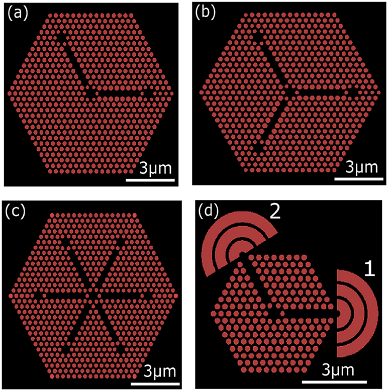
Figure 1. Schematic of the structure having multiple cavities coupled by waveguides for: 2-way (a), 3-way (b), 6-way (c) structures and with the ring couplers [labeled as 1 and 2 in (d)] for out of plane coupling of field. Photonic crystal structures consist of air holes (Red circles) in GaAs film (black).
Numerical Modeling and Analysis
The structure consists of air holes (red circles) in GaAs film (black region) as shown in Figures 1a–d. For simulating these structures, we used Full-Wave numerical simulation software Lumerical [24] to implement finite difference time domain (FDTD). GaAs is chosen as the substrate and the material parameters given by Palik [25] have been used for simulation. We considered wafer parameters with 150 nm GaAs in the suspended air-bridge geometry with air at the top and bottom of the GaAs [10, 12]. This gives vertical (out of plane) confinement of the field. While air is at the top, the bottom air gap is realizable with a sacrificial AlGaAs layer below the 150 nm thick GaAs film such that the molecular beam epitaxy grown wafer profile is, GaAs (150 nm)–AlGaAs (1 μm)–GaAs (Buffer layer)–GaAs (substrate). The perfectly matched layer (PML) boundary condition has been used in the out of plane geometry [26].
The mesh size is taken to be 20 nm, about a/18 where a is the lattice constant (a = 360 nm). The mesh is conformal. The simulation time is 10 ps to simulate ~11 x 11 μm area PC structure. The PC structures consist of hexagonal lattice of air holes embedded in GaAs substrate. The air-bridge structure is created with air as cladding on the top and bottom. We have used two types of monitors: Frequency domain field and power monitor and time monitor to determine the transmission spectra, transmission efficiency and resonance wavelengths. Frequency domain field and power monitor gives us the field intensity in a range of frequencies. Frequency-domain field monitors collect CW, steady state EM field data in the frequency domain from an FDTD or variable FDTD simulation. Based on the observations, we determined the coupling efficiency, electric field intensity profile, transmission spectra, and the resonance wavelength. The time monitors provide us with time-domain information for field components over the course of the simulation. These are used for extracting the line widths of resonances through Fourier analysis and thus, are useful in calculating the Q factor and coupling efficiency.
The proposed demultiplexer/splitter has three main components: the input cavity, the waveguide section and the output cavity. Both the input and output cavities are H1 cavities which are formed by removing a central air hole and varying the radii and position of adjoining air holes. Optimization is done to achieve high q-factor of the cavity and match the emission wavelength of GaAs/InGaAs quantum dot emission. The quantum dot (QD) emission in the input cavity is simulated by a dipole source at this location covering the wavelength range of 900–1,300 nm. To study polarization dependence and also to mimic the Zeeman split levels, one can use two orthogonally polarized dipole sources [10]. As is well-known, in the H1 cavity, the cavity mode depends on: (1) radii (r1) of the adjacent air holes (as r1 increases, λ decreases), and (2) outward shift (Δ1) of the adjacent air holes which determines the extent of confinement of a particular mode.
The waveguides couple light from input to the output resonant cavity. The coupling efficiency is controlled by manipulating the evanescent field coupling between the cavities and the waveguides. From design perspective, coupling efficiency as well as operation (whether optical splitter or DEMUX), depends on (a) input cavity parameters, (r1, a1 (a1 = a + Δ1)), (b) output cavity parameters, (r2, a2 (a2 = a + Δ2)) (c) radii of air holes adjacent to the line defect (w1/2/3), i.e., the waveguide parameters and d) the length of the waveguide. This is illustrated in Figure 2 (Δ1, Δ2 is the outward shift of the air holes constituting the H1 cavity). Airholes marked h, plays a key role in improving the coupling efficiency.
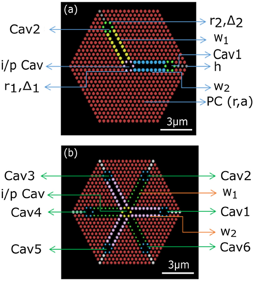
Figure 2. (a) Schematic for 2-way optical power splitter made by making air holes (different color circles) in GaAs (black). (b) Schematic for 6-way optical power splitter. Different color of the air holes indicate different radius of the holes. Each hole size is optimized to maximize the coupling efficiency.
The point defect breaks the symmetry of the crystal and therefore allows out-of-plane coupling. At the input cavity, energy is excited by the presence of orthogonal dipole sources, while at the output cavity the energy is picked up for analysis. Since the size of output cavity (~1 × 1 μm) is very small, ring couplers (as shown in Figure 1d) are used to collect the out-coupled energy from the PC [27].
Simulation Results
Photonic crystal structures shown in Figures 1, 2 were optimized by a multi-level process beginning with first determining the radius of air holes (r) and lattice constant (a) of the PC such that the bandgap lies around λ = 1 μm, which is the emission wavelength of GaAs/InGaAs quantum dots which we are interested in Masumoto and Takagahara [28]. The corresponding r and a are found to be r = 0.13 μm, and a = 0.36 μm, such that r/a = 0.361 for the regular air holes. Further, to optimize the Q factor of the H1 cavity, we removed the central air hole and shifted the next nearest air holes outwards by Δ. This Δ is same for both input and output cavities and is varied between ±0.1 a. To optimize the structure for high transmission efficiency, low cross-talk, low channel separation and low footprint, role of several parameters is systematically studied such as, the size of air holes in the input H1 cavity, waveguide, output H1 cavity as well as all those labeled in Figure 2. In Figure 2 different size holes are marked by different colors.
By systematic investigation all the PC parameters were optimized. We began with the parameters of input cavity (r1, a1) followed by optimizing the parameters of output cavity (r2, a2). The waveguide is created by removing a line of air holes and then varying the radii of the nearby air holes to form the line defect i.e., effectively optimizing the waveguide width, followed by optimizing the waveguide length. Finally coupling efficiency is enhanced by modifying the airholes marked “h.” The hexagonal symmetry of the PC is undisturbed by creating Y-waveguides with angular separation which is integral multiple of 60°. Earlier maximum cavity-waveguide coupling was reported when the cavity and waveguide were oriented at 60° to each other such that the evanescent tails of the cavity and the waveguide are oriented [23]. In our case, while retaining the hexagonal geometry of the lattice, we optimize the structural parameters including the radii of air holes marked “h,” to achieve high coupling. The final optimization of r1, r2, w1, w2, w3, and h is achieved by varying the parameters from 0.38 to 1.15 r. The optimized parameters and the corresponding transmission efficiencies for r = 130 nm and a = 360 nm are listed in the Appendix under Tables A1–A3.
The main resonance with the highest Q factor is at 1.004 μm. The electric field profile at different heights for this resonance are shown in Figures 3a–c. Figure 3a shows the field at the center of the 150 nm thick GaAs film. Figure 3b shows the electric field profile at a height 400 nm above the GaAs film showing the vertical coupling. Electric field profile at the central cavity (zoom in of Figure 3a) is shown in Figure 3c. In addition to this main resonance, there are 6 more resonances found for this structure. Transmission spectrum as well as the electric field profiles at other resonances are shown in Figures 4a–g. The resonances are labeled in Figure 4a as, (1) λ = 945 nm, (2) λ = 985 nm, (3) λ = 1,004 nm, (4) λ = 1,009 nm,(5) λ = 1,059 nm, (6) λ = 1,072 nm, and (7) λ = 1,086 nm. The electric field profiles (Figures 4b–g) clearly show that not all the resonances are suitable for splitter function. So, depending on the calculated field profiles and the efficiency we chose a particular resonance for a particular functionality.
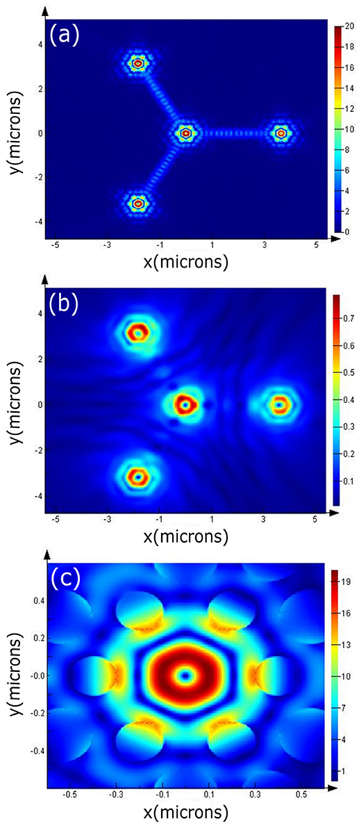
Figure 3. (a) Electric field profile for a 3–way splitter at λ ~ 1.004 μm at the middle of the 150 nm thick GaAs patterned film (b) Electric field profile at 400 nm above the sample surface showing out of plane coupled field from the cavity regions. (c) Electric field profile of the hexapole mode at the central cavity shown in (a).
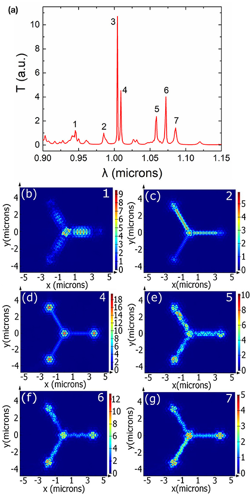
Figure 4. (a) Transmission spectra of 3-way optical splitter with different resonances marked 1–7. (b–g) show the electric field profile at different resonances (labeled on right top of each figure). Electric field profile for resonance labeled 3 is shown in Figure 3a.
While designing a 6-way demultiplexer/splitter we have not modified each of the waveguide dimensions independently, instead we have split them into two groups that are angled from each other by 60° as illustrated in Figure 2 (different color schemes are adopted to indicate the two sets of waveguides whose parameters w1, and w2 are varied to achieve the desired functionality–DEMUX or splitter).
It is observed that as the cavity size decreases (i.e., as the radii r1, and r2 increases) or as the waveguide narrows (w1/2/3 increases) there is a blue shift of the resonance. The optimized waveguide length (lwg) is 2.52 μm. The cavity gets coupled to leaky modes which can cause radiation losses. Figure 3 shows the calculated electric field profile at different positions, on the surface of the crystal as well as above the crystal, which can be experimentally studied using near field optical scanning microscopes.
While studying resonance we have spanned a broad range of frequencies (0.9–1.15 μm, as illustrated in Figure 4a) and different resonances can be observed. However, the resonances near 1 μm are chosen so that it matches with the InAs QD emission for which the structures are being designed [29]. For example, a 3-way optical splitter shows good coupling at λ = 1.004, 1.009, and 1.072 μm as illustrated in Figures 3a, 4d,f, respectively. However, λ = 1.004 μm shows the highest coupling efficiency and thus is chosen over the other two resonances.
Ring Coupler
Efficient out coupling of the field with minimal polarization distortion is also important for practical use of the designs presented. Toward this, we optimized ring couplers at the end of each waveguide. Figure 1d shows the schematic of the ring coupler to couple light from the PC waveguide out of the plane of the crystal. The ring coupler consists of 3 rings with a pitch given by, λ /(2n) ~140 nm (λ ~ 955 nm, nGaAs = 3.4) The ring coupler is offset from the output port of the waveguide by λ /(2n) [27] as shown in the schematic of Figure 1d. FDTD was used to verify the scattering properties of the ring coupler. Figure 5 plots the electric field profile of the resonance, illustrating the out coupled light in the z-direction at different heights above the surface. The coupling efficiency is determined by comparing the in-plane electric field intensity at the ring coupler to that of the input cavity. The coupling efficiency for the ring coupler (calculated at the surface of the substrate) at Ports 1 and 2 (labeled in Figure 1d) is 8.4 and 24.8%, respectively. The coupling efficiency of the couplers depends on the ring parameters, ring thickness, and the air gap separating the rings.
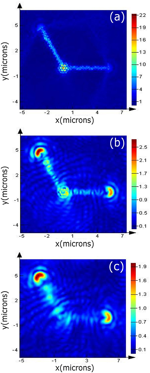
Figure 5. Electric field profile to show the response of ring couplers with monitors kept at different heights, (a) on the surface of the structure (b) at 200 nm above the structure, and (c) at 400 nm above the structure.
While the designs offer smallest footprint reported so far for DEMUX or splitting functions, the challenges in practically realizing these structures is the ability to place a quantum dot (light source is considered as a dipole source in the input cavity) at the field maxima point inside the central cavity. One way to place the QD at the center of the cavity is to use an atomic force microscope (AFM) tip to pick a colloidal QD and place it at the required position. However, such QD positioning methods are stochastic and needs to be checked for the presence of a luminescent QD at the desired location. Out-of-plane scattering as well as in-plane scattering are the sources of losses in PC structures. In addition, the input and output coupling losses and the scattering due to inhomogeneity in the hole size and shape in fabricated structures limit the efficiency of the PC structures.
Conclusion
We propose to use various resonant modes in a coupled cavity—waveguide structure on a GaAs/InAs/GaAs QD wafer to realize 2-, 3-, and 6-way optical demultiplexer and splitter. The structures are optimized by detailed FDTD simulations by studying the dependence of the air hole dimensions of input cavity, output cavity as well as the waveguide parameters. The structures designed are promising with a very small footprint of 78 μm2, much smaller than those reported so far. The advantages of these structures are ease of fabrication, broad spectral coverage by modifying the structural parameters and high transmission power. These are suitable for far-field excitation of quantum dots placed inside the input cavity and coupling the emission to various channels through the waveguide coupled output cavities. Thus, these are suitable for quantum information studies as well.
Author Contributions
VA conceived the idea. RG and BN did the simulations. VA, RG, BN, and AT discussed the results and prepared the manuscript.
Conflict of Interest Statement
The authors declare that the research was conducted in the absence of any commercial or financial relationships that could be construed as a potential conflict of interest.
Acknowledgments
Department of Science and Technology, Government of India for financial support to RG through grant number SR/ WOS-A/ET- 86/2013.
Supplementary Material
The Supplementary Material for this article can be found online at: https://www.frontiersin.org/articles/10.3389/fphy.2018.00152/full#supplementary-material
References
1. Park J, Baik J, Lee C. Fault-detection technique in a WDM-PON. Opt Express (2007) 15:1461–6. doi: 10.1364/OE.15.001461
2. Mun SG, Moon JH, Lee HK, Kim JY, Lee CH. A WDM-PON with a 40 Gb/s (32 × 1.25 GB/s) capacity based on wavelength-locked Fabry–Perot laser diodes. Opt Express (2008) 16:11361–8. doi: 10.1364/OE.16.011361
3. Ortega B, Mora J, Puerto G, Capmany J. Symmetric reconfigurable capacity assignment in a bidirectional DWDM access network. Opt Express (2007) 15:16781–6. doi: 10.1364/OE.15.016781
4. Soltani M, Haque A, Momeni B, Adibi A, Xu Y, Lee RK. Designing complex optical filters using photonic crystal microcavities. Proc SPIE (2003) 5000:257–65. doi: 10.1117/12.480062
5. O'Brien JL. Furusawa A, Vučković J. Photonic quantum technologies. Nat Photon (2009) 3:687–95. doi: 10.1038/nphoton.2009.229
6. Thompson MG, Politi A, Matthews JCF, O'Brien JL. Integrated waveguide circuits for optical quantum computing. IET Circuits Devices Syst. (2011) 5:94–102. doi: 10.1049/iet-cds.2010.0108
7. Orieux A, Diamanti E. Recent advances on integrated quantum communications. J Opt. (2016) 18:083002. doi: 10.1088/2040-8978/18/8/083002
8. Elshaari AW, Zadeh IE, Fognini A, Reimer ME, Dalacu D, Poole PJ, et al. On-chip single photon filtering and multiplexing in hybrid quantum photonic circuits. Nat Commun. (2017) 8:379. doi: 10.1038/s41467-017-00486-8
9. Harris NC, Bunandar D, Pant M, Steinbrecher GR, Mower J, Prabhu M, et al. Lage scale quantum photonic circuits in silicon. Nanophotonics (2016) 5:456–68. doi: 10.1515/nanoph-2015-0146
10. Luxmoore IJ, Wasley NA, Ramsay AJ, Thijssen ACT, Oulton R, Hugues M, et al. Semiconductor waveguide circuit for coupling an InGaAs quantum dot spin to a path encoded photon. Phys Rev Lett. (2013) 110:037402. doi: 10.1103/PhysRevLett.110.037402
11. Liu HY, Lan S, Wu LJ, Guo Q, Hu W, Liu SH, et al. Self-induced anderson localization and optical limiting in photonic crystal coupled cavity waveguides with Kerr nonlinearity. Appl Phys Lett. (2007) 90:213507. doi: 10.1063/1.2742595
12. Goel R, Vengurlekar AS, Achanta VG, Ramsay AJ. Photonic crystal based polarization beamsplitter. In: IEEE International Conference on Nanoscience, Technology and Societal Implication- NSTSI. Bhubaneswar (2011). doi: 10.1109/NSTSI.2011.6111803
13. Goel R, Tulapurkar A, Achanta VG. Photonic crystal based coupled cavity structure for scalable quantum circuits. In: 12th International Conference on Fiber Optics and Photonics, Optical Society of America, paper M4A.84. Kharagpur (2014). doi: 10.1364/PHOTONICS.2014.M4A.84
14. Bernier D, Roux XL, Lupu A, Marris-Morini D, Vivien L, Cassan E. Compact low crosstalk CWDM demultiplexer using photonic crystal superprism. Opt Express (2008) 16:17209–14. doi: 10.1364/OE.16.017209
15. Momeni B, Huang J, Soltani M, Askari M, Mohammadi S, Rakhshandehroo M, et al. Compact wavelength demultiplexing using focusing negative index photonic crystal superprisms. Opt Express (2006) 14:2413–22. doi: 10.1364/OE.14.002413
16. Cheng SC, Wang JZ, Chen LW, Wang CC. Multichannel wavelength division multiplexing system based on silicon rods of periodic lattice constant of hetero photonic crystal units. Optik (2012) 123:1928–33. doi: 10.1016/j.ijleo.2011.09.036
17. Rostami A, Nazari F, Alipour-Banaei H, Bahrami A. A novel proposal for DWDM demultiplexer design using modified-T photonic crystal structure. Phot. Nanostruct Fundam Appl. (2010) 8:14–22. doi: 10.1016/j.photonics.2009.12.002
18. Rostami A, Alipour-Banaei H, Nazari F, Bahrami A. An ultracompact photonic crystal wavelength division demultiplexer using resonance cavities in a modified Y-branch structure. Optik (2011) 122:1481–85. doi: 10.1016/j.ijleo.2010.05.036
19. Rakhshani MR, Mansouri-Birjandi MA. Design and simulation of wavelength demultiplexer based on heterostructure photonic crystals ring resonators. Physica E (2013) 50:97–101. doi: 10.1016/j.physe.2013.03.003
20. Alipour-Banaei H, Mehdizadeh F, Hassangholizadeh Kashtiban M. A novel proposal for all optical PhC-based demultiplexers suitable for DWDM applications. Opt Quant Electron (2013) 45:1063–75. doi: 10.1007/s11082-013-9717-x
21. Mehdizadeh F, Soroosh M. A new proposal for eight-channel optical demultiplexer based on photonic crystal resonant cavities. Photon Netw Commun. (2016) 31:65–70. doi: 10.1007/s11107-015-0531-1
22. Mock A, Lu L, O'Brien J. Space group theory and fourier space analysis of two-dimensional photonic crystal waveguides. Phys Rev B (2010) 81:155115. doi: 10.1103/PhysRevB.81.155115
23. Faraon A, Waks E, Englund D, Fushman I, Vučković J. Efficient photonic crystal cavity-waveguide couplers. Appl Phys Lett. (2007) 90:073102. doi: 10.1063/1.2472534
26. Taflove A, Hegnese SC. Computational Electrodynamics: The Finite-Difference Time-Domain Method. Boston, MA: Artech House (1998).
27. Faraon A, Fushman I, Englund D, Stoltz N, Petroff P, Vučković J. Dipole induced transparency in waveguide coupled photonic crystal cavities. Opt Express (2008) 16:12154–62. doi: 10.1364/OE.16.012154
28. Masumoto Y, Takagahara T. Semiconductor Quantum Dots: Physics, Spectroscopy and Applications. Berlin: Springer Science & Business Media (2013). doi: 10.1007/978-3-662-05001-9
29. Goel R, Nayak BK, Maurya S, Tulapurkar A, Achanta VG. Photonic crystal microcavities with quantum dot defect: toward quantum information processing. In: 13th International Conference on Fiber Optics and Photonics. Optical Society of America, paper W2E.3, Kanpur (2016). doi: 10.1364/PHOTONICS.2016.W2E.3
Keywords: dense wavelength division multiplexing (DWDM), demultiplexer, optical splitter, footprint, quantum dot
Citation: Goyal R, Nayak BK, Tulapurkar A and Achanta VG (2019) Photonic Crystal Based 2/3/6- Way Optical Splitter and Demultiplexer. Front. Phys. 6:152. doi: 10.3389/fphy.2018.00152
Received: 05 September 2018; Accepted: 12 December 2018;
Published: 08 January 2019.
Edited by:
Yanpeng Zhang, Xi'an Jiaotong University, ChinaReviewed by:
Weifeng Zhang, University of Ottawa, CanadaVenugopal Rao Soma, University of Hyderabad, India
Copyright © 2019 Goyal, Nayak, Tulapurkar and Achanta. This is an open-access article distributed under the terms of the Creative Commons Attribution License (CC BY). The use, distribution or reproduction in other forums is permitted, provided the original author(s) and the copyright owner(s) are credited and that the original publication in this journal is cited, in accordance with accepted academic practice. No use, distribution or reproduction is permitted which does not comply with these terms.
*Correspondence: Venu Gopal Achanta, achanta@tifr.res.in
 Richa Goyal1,2
 Ashwin Tulapurkar
 Venu Gopal Achanta