 Yang Xu
 Fanming Huang
 Wenwu Li
- Engineering Research Center of Nanophotonics and Advanced Instrument (MOE), Technical Center for Multifunctional Magneto-Optical Spectroscopy (Shanghai), School of Physics and Electronic Science, East China Normal University, Shanghai, China
Despite the intensive study on the promotion of device performance, the device physics regarding the effects of Schottky barrier on the charge injection in conjugated polymer transistors still need more discussions. Here, the indacenodithiophene–co-benzothiadiazole (IDT-BT) organic field-effect transistors (OFETs) with four different contact metals (Pt, Au, Cu, and Cr) were fabricated to explore the effects. Different Schottky barriers were achieved with the contact electrode’s work function (WF) varying. The ION/IOFF ratio of IDT-BT OFETs increases from 103 to 106 as the WF increases from 4.6 to 5.65 eV. The hole mobility also increases from 0.01 (for Cr) to 2.79 cm2V–1s–1 (for Pt) when the WF approaches the highest occupied molecular orbital (HOMO) level of the conjugated polymer. Moreover, the threshold voltage and subthreshold swing of the devices both decrease with increasing the WF. These could be ascribed to the lowered Schottky barrier with WF, which promotes charge injection. The lowest Schottky barrier (0.123 eV) and contact resistance (1.06 × 10⁴ Ω⋅cm) can be achieved in the devices with Pt contacts, owing to the highest work function.
Introduction
Solution-processed organic field-effect transistors (OFETs) are promising for next-generation consumer electronics, because of the unique advantages of low cost, flexibility, and large-area fabrications (Liu et al., 2010; Jiang et al., 2019). In order to improve the device performance for applications, much efforts have been paid to the material synthesis, film microstructure, device fabrication, and charge transport optimization of OFETs (Chen et al., 2012; Yuan et al., 2014; Uemura et al., 2016). Among these researches, charge injection, which occurs at the interface between metal and organic semiconductor (OSC), is one of the key factors to promote the device performance. Due to the presence of the Schottky barrier, charge injection can be significantly limited. According to the Schottky–Mott limit, the Schottky barrier height can be roughly estimated from the difference between the contact electrode’s work function (WF) and the transporting energy level of the OSC (Tang et al., 2016).
On the other hand, the contact resistance (RC) of OFETs is very high, which is due to the absence of doping as well as the heterogeneous materials at the electrode–semiconductor junction (Liu et al., 2015). With the channel length reducing, the RC impact is amplified, further degrading the charge injection (Choi et al., 2018; Wang et al., 2018). Therefore, the relationship between the charge injection and the device characteristics needs to be investigated in detail. The WF of these four contact metals is 5.65, 5.10, 4.65, and 4.60 eV, respectively. So different heights of Schottky barriers can be formed in IDT-BT OFETs, which will help us to systematically explore the Schottky-barrier-dependent electrical characteristics.
In this work, the Schottky barrier, the RC, and charge injection in indacenodithiophene–co-benzothiadiazole (IDT-BT) OFETs with four different contact metals (Pt, Au, Cu, and Cr) were studied. The effects of the Schottky barrier on the performance parameters such as the mobility, the threshold voltage (VTH), and subthreshold swing (SS) have also been explored.
Device Fabrication and Characterizations
The device structure of the top-gate staggered IDT-BT transistors and the molecular structure of IDT-BT polymer are shown in Figures 1A,B. The drain and source electrodes of different metals (Pt, Au, Cu, and Cr) with thickness of 30 nm were made on pre-cleaned Corning glass substrate by magnetron sputtering through shadow mask. The channel width (W) was fixed to 1200 μm while the channel length (L) varies from 60 to 350 μm. The conjugated polymer, IDT-BT, dissolved in dichlorobenzene (8 mg/mL) was spin-coated at 2000 r/min in argon-fill glove box and then annealed in the same glove box at 100°C for 1 h. Subsequently, polystyrene dissolved in butyl acetate (80 mg/mL) was spin-coated at 2000 r/min as the gate dielectric and then annealed at 80°C for 12 h. Finally, the top gate electrodes of Al (80 nm) were prepared by thermal evaporation through shadow mask. The thicknesses of the IDT-BT semiconductor and PS dielectric layer were estimated to about 50 and 1000 nm, respectively. The electrical properties of the fabricated IDT-BT OFETs were characterized at the temperature of 100–280 K by using probe station (Lakeshore TTPX) equipped with semiconductor parameter analyzer (Keithley 4200-SCS).
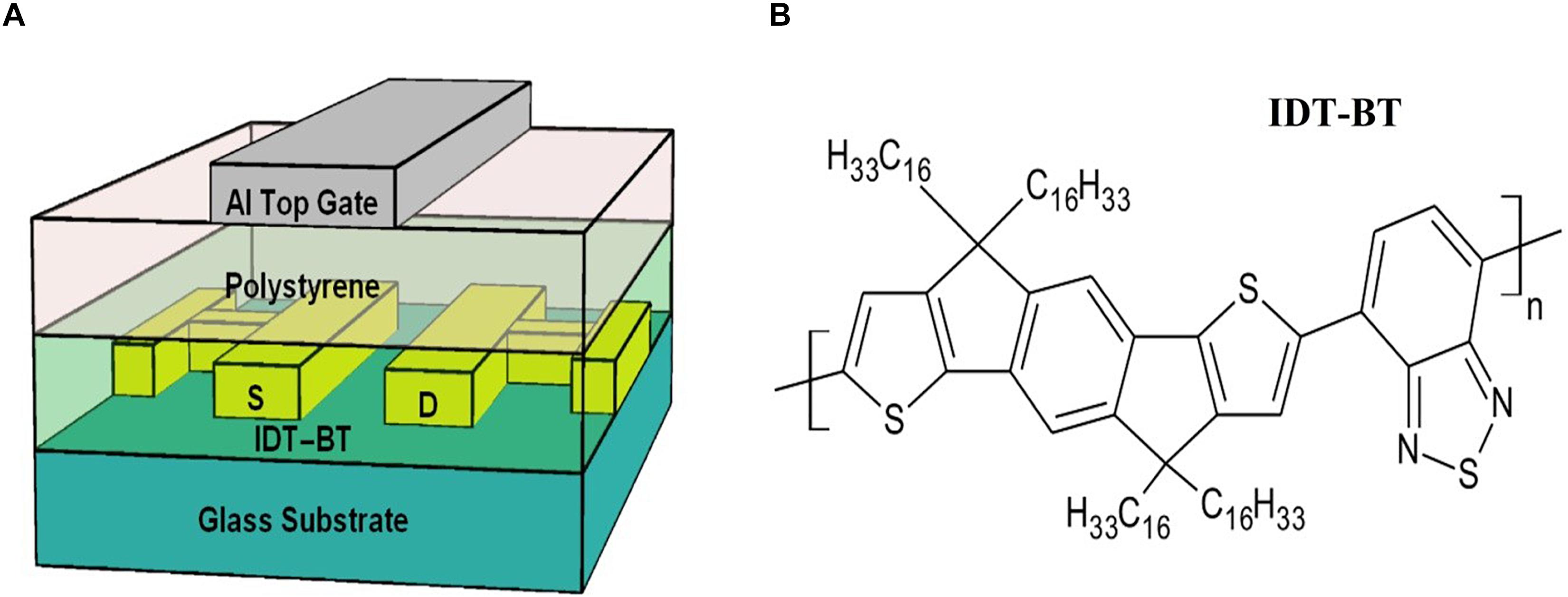
Figure 1. (A) Schematic illustration of the device structure of top-gated IDT-BT OFETs. (B) Molecular structure of IDT-BT polymer.
Results and Discussion
On–Off Ratio Analysis
Figures 2A,B show the typical saturation and linear transfer characteristics of the devices with four different contact metals (where W/L = 1200/60 μm). In the saturation regime (at the drain voltage VD = -100 V), the ION/IOFF ratio constantly increases from 103 to 104, 105, and 106 for the transistors with Cr, Cu, Au, and Pt contacted, respectively, mainly due to the rising on-state drain current (ID) that augments from 10–6 A (Cr contact) to 10–4 A (Pt contact). The result is consistent with the lower Schottky barrier for higher work-function metal adopted in the OFETs, as predicted by the Schottky–Mott limit where the Schottky barrier equals to the energy difference between the metal’s work function (WF) and the highest occupied molecular orbital (HOMO) level of the OSC.
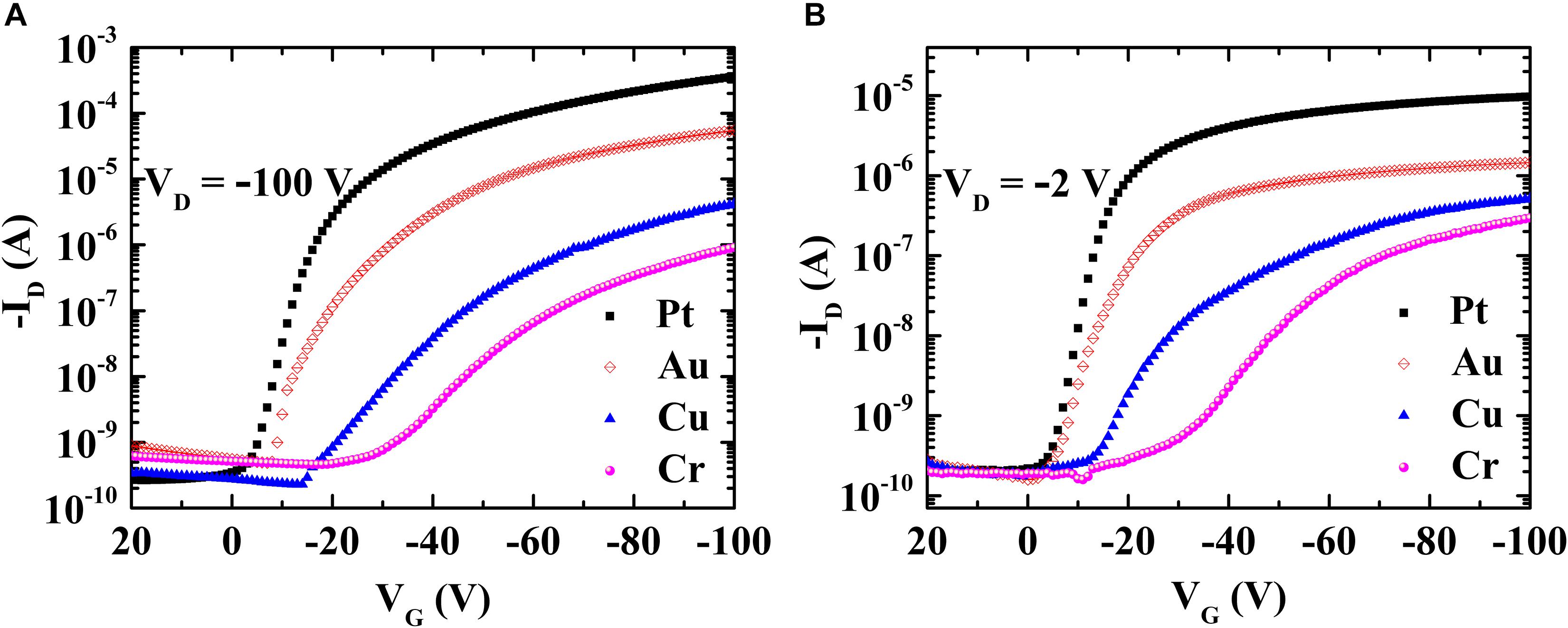
Figure 2. (A) Saturation and (B) linear transfer curves of the IDT-BT OFETs with four different contact metals Pt, Au, Cu, and Cr, respectively.
Key Electrical Parameters of Devices
The key electrical parameters are summarized in Table 1. The rising on-state current suggests the promotion of the mobility. The saturation field-effect mobility (μSAT) is thus calculated from the saturation regime by using the following equation:
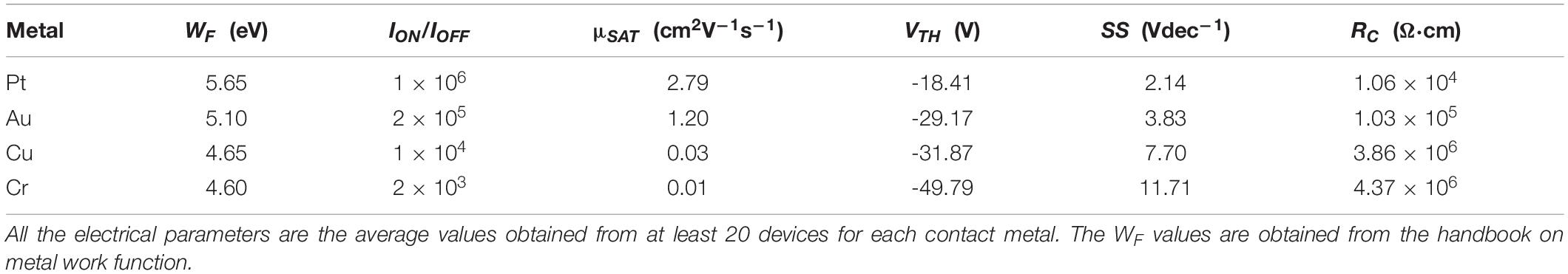
Table 1. The key electrical parameters of IDT-BT OFETs with four different contact metals.
where L, W, ID, VG, and CINS are the channel length, channel width, drain current, gate voltage, and unit-area gate capacitance of the gate dielectric, respectively (Uemura et al., 2016). As listed in Table 1, the μSAT constantly increases from 0.01 to 0.03, 1.20, and 2.79 cm2V–1s–1 for the OFETs with Cr, Cu, Au, and Pt contacts, respectively. The IDT-BT OFETs with Pt electrodes show the highest mobility (2.79 cm2V–1s–1). It is two times higher than the mobility of IDT-BT OFETs with Au electrodes (Shin et al., 2017; Wang et al., 2017). This value is even higher than the devices with Cu and Cr electrodes by two orders of magnitude. This result indicates that the contact metals with different WF can indeed significantly affect the device performance by altering charge injection. The examination of the literature shows that the WF of Pt is 5.65 eV, which is nearest to the HOMO level of IDT-BT (5.4 eV) (Xu et al., 2017). Hence, the Schottky barrier for Pt contact OFETs is 0.25 eV, which is beneficial for the hole injection from the electrode to the channel. For the other three metals, the value is at least 0.3 eV. The energy barriers are really high, so the hole injection from the source electrodes into channel is difficult. Therefore, the charge transport and the electrical performance of the OFETs are deteriorated.
The sub-threshold swing (SS) and the threshold voltage (VTH) reflect the influence of the Schottky barrier (Jiang et al., 2019). This is because the charge injection can also be limited by high Schottky barrier that is not directly or not efficiently modulated by the gate voltage. Thus, it leads to slow and late charge accumulation, i.e., large SS and high VTH. Note that small SS and VTH are desirable for practical applications especially for high-speed operation and low-power consumption (Lai et al., 2018; Wei et al., 2018). From Table 1, we can find that the SS and VTH values monotonically decrease with increasing the contact’s WF, indicating the improved charge injection. Furthermore, the electrical parameters can be modulated with different heights of Schottky barrier. High Schottky barrier was formed, when the WF difference between the contact metal and the HOMO level of IDT-BT is large. It will further lead to poor charge injection and non-ohmic contacts. On the other hand, a nearly ohmic contact is expected, when the WF of the contact metal approaches the HOMO level of IDT-BT. It will promote the charge injection and accumulation (Ishii et al., 1999).
Effect of Contact Metals on Contact Resistance
Due to the absence of doping in OFETs, the contacts between metal and OSC are basically Schottky contacts with great barrier height. The contact resistance (RC) is usually very high, which is a critical issue to OFETs (Liu et al., 2015). The transfer line method (TLM) can be adopted to extract the Rc of the IDT-BT OFETs. In the linear regime, the total resistance (RTOT) can be written as the sum of the RC and channel contact (RCH) according to:
where VD is the drain voltage. The RC is independent on the channel length (L), while the RCH proportionally declines with reducing L. Therefore, for a fixed VG, when RTOT is plotted against L, a straight line can be obtained with whose y-axis intercept is RC (Natali and Caironi, 2012). For our devices, the contact resistance normalized by the channel width (RC × W) is shown in Figure 3. Note that the RC is clearly lower for the Au and Pt contacted OFETs, compared to Cu and Cr contacted devices. A lowest value of 1.06 × 10⁴ Ω⋅cm is obtained for Pt-based devices at the VG of −80 V. The RC increases to 1.03 × 10⁵ Ω⋅cm for the OFETs with Au electrodes, and then markedly increases to 3.86 × 10⁶ and 4.37 × 10⁶ Ω⋅cm for that with Cu and Cr electrodes, respectively (Huang et al., 2019). Such high RC may dominate the RTOT in particular when L is short because the RCH proportionally declines with reducing L while the RC does not. So, the overall device properties can be governed by the contact properties (Xu et al., 2017). As a result, largely overestimated mobility may be caused. Only the channel is sufficiently long to ensure the insignificant contact impact so as to extract accurate mobility (Liu et al., 2017). The charge injection is difficult, when the RC is large. So the drain current is suppressed and the electrical characteristics of the device are deteriorated. When the RC is low, the charges, only need a small energy, can pass through the barrier at the interface of electrode and semiconductor. Furthermore, charge accumulation will be quickly and easily occurred for the OFETs with lower RC. Therefore, the charge injection is strong, resulting the high performance of IDT-BT OFETs.
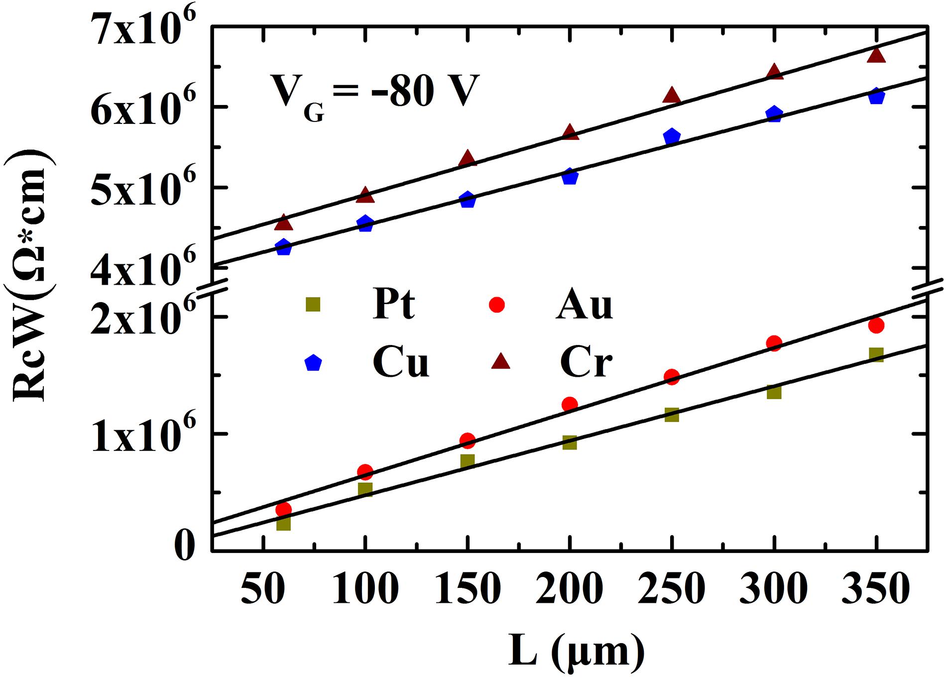
Figure 3. The normalized contact resistance (RC × W) and the linear fitting results of top-gated IDT-BT OFETs with different channel length and with Pt, Au, Cu, and Cr contact metal, respectively.
Intrinsic Schottky Barrier of Pt- and Au-Based OFETs
Figures 4A,B show the output characteristics measured at different temperatures (T). According to the thermionic emission, the saturation current of a reverse-biased Schottky junction can be calculated from Eq. (3):
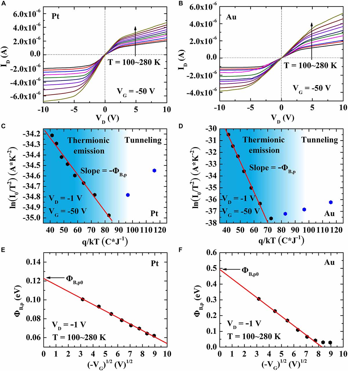
Figure 4. Output characteristics of top-gated IDT-BT OFETs with (A) Pt and (B) Au contacts at the temperatures varying from 100 to 280 K; linear fit for the thermionic emission model for the devices with (C) Pt and (D) Au contacts. The Schottky barrier (ΦB) is extracted from the slope of the linear fitting of ln(I0/T2) versus (q/kT) curve; linear fit for the image-force barrier lowering arising from VG for the devices with (E) Pt and (F) Au contacts. An intrinsic barrier (ΦB,p0) is obtained by the intercept at zero VG, where VD = −1 V.
where A is the diode area, A∗ is the Richardson constant, T is the absolute temperature, q is the elementary charge, ΦB is the height of the Schottky barrier, and k is the Boltzmann constant (Rhoderick and Williams, 1988). Therefore, through the output characteristics at variable temperatures, ΦB can be extracted from the plot of ln(I0/T2) versus (q/kT). The Pt-based and Au-based devices (measured at VD = -1 V and VG = -50 V) clearly show such a dependency (Figures 4C,D). The ΦB value can be extracted form the slope of the linear fitting of ln(I0/T2) versus (q/kT) curve (Xu et al., 2017). Because the image-force barrier lowering is significant in OFETs, which makes ΦB highly dependent on the external biases (Bartolomeo et al., 2018), linear fitting of ΦB is made against VG (at small VD = -1 V) to eliminate the associated effect (Brondijk et al., 2012), as seen in Figures 4E,F. The intrinsic Schottky barriers without biasing influence (ΦB,p0) of 0.123 and 0.487 eV are obtained for Pt-based and Au-based devices, respectively. These values are different from the theoretical prediction given by the Schottky–Mott limit, due to the different interface chemistry and physics (Xu et al., 2017). The interface of electrode and semiconductor exhibits an additional dipole barrier that tends to change the WF and hence the interface barrier height (Wan et al., 2005). Furthermore, gap states, which can be easily generated in OFETs, are also major influences on Schottky barrier. The hopping ladder and Fermi-level pinning occur and thus the charge injection through the Schottky barrier is limited (Tung, 2000). Despite that, one can still draw conclusion. The minor ΦB,p0 = 0.123 eV means nearly ohmic contacts formed in Pt-based devices, where the charge injection is efficient. By contrast, the high Schottky ΦB,p0 = 0.487 eV means that the charge injection in Au-based devices is by low-efficiency thermionic emission over high energy barrier. Therefore, the different Schottky barriers lead to different charge injection mechanisms and thus giving rise to very different electrical characteristics.
Conclusion
Schottky-barrier-dependent electrical properties of the transistors using conjugated polymer of IDT-BT and four contact metals have been presented. It is found that the contact’s work function changes the Schottky barrier height, alternating the mechanism of charge injection. A highest mobility of 2.79 cm2V–1s–1 and lowest RC of 1.06 × 10⁴ Ω⋅cm are observed from Pt-based devices, attributable to the nearly ohmic contacts with a small Schottky barrier ΦB,p0 = 0.123 eV. This well explains the greatly improved ION/IOFF ratio, VTH, and SS. Therefore, our results demonstrate that Schottky barrier is crucial for performance optimization to achieve practical organic devices and circuits.
Data Availability Statement
The datasets generated for this study are available via the corresponding author or other researchers following publication.
Author Contributions
The project was initiated by WL. YX performed the experiments. YX, FH, and WL prepared the figures and manuscript.
Funding
This work was supported in part by the National Key Research and Development Program of China (Grant No. 2016YFB0501604), the Natural Science Foundation of China (Grant Nos. 61774061 and 61504043), the Natural Science Foundation of Shanghai (Grant No. 19ZR1473400), the NSAF foundation of China (Grant No. U1830130), and the ECNU Academic Innovation Promotion Program for Excellent Doctoral Students (Grant No. YBNLTS2019-028).
Conflict of Interest
The authors declare that the research was conducted in the absence of any commercial or financial relationships that could be construed as a potential conflict of interest.
References
Bartolomeo, A. D., Grillo, A., Urban, F., Iemmo, L., Giubileo, F., Luongo, G., et al. (2018). Asymmetric schottky contacts in bilayer MoS2 field effect transistors. Adv. Funct. Mater. 28:1800657. doi: 10.1002/adfm.201800657
Brondijk, J. J., Torricelli, F. E., Smits, C. P., Blom, P. W. M., and Leeuw, D. M. (2012). Gate-bias assisted charge injection in organic field-effect transistors. Org. Electron. 13, 1526–1531. doi: 10.1016/j.orgel.2012.04.029
Chen, Z., Lee, M. J., Ashraf, R. S., Gu, Y., Seifried, S. A., Nielsen, M. M., et al. (2012). High-performance ambipolar diketopyrrolopyrrole-thieno[3,2-b]thiophene copolymer field-effect transistors with balanced hole and electron mobilities. Adv. Mater. 24, 647–652. doi: 10.1002/adma.201102786
Choi, H. H., Rodionov, Y. I., Paterson, A. F., Panidi, J., Saranin, D., Kharlamov, N., et al. (2018). Accurate extraction of charge carrier mobility in 4-probe field-effect transistors. Adv. Funct. Mater. 28:1707105. doi: 10.1002/adfm.201707105
Huang, F. M., Liu, A., Zhu, H. H., Xu, Y., Noh, Y., Li, W. W., et al. (2019). Reliable mobility evaluation of organic field-effect transistors with different contact metals. IEEE Electron Device Lett. 40, 605–608. doi: 10.1109/LED.2019.2901315
Ishii, H., Sugiyama, K., Ito, E., and Seki, K. (1999). Energy level alignment and interfacial electronic structures at organic/metal and organic/organic interfaces. Adv. Mater. 5, 605–625. doi: 10.1002/(SICI)1521-4095(199906)11
Jiang, C., Choi, H. W., Cheng, X., Ma, H., Hasko, D., and Nathan, A. (2019). Printed subthreshold organic transistors operating at high gain and ultralow power. Science 363, 719–723. doi: 10.1126/science.aav7057
Lai, S., Jang, S. K., Cho, J. H., and Lee, S. (2018). Organic field-effect transistors integrated with Ti2CTx electrodes. Nanoscale 10, 5191–5197. doi: 10.1039/C7NR08677F
Liu, C., Li, G., Pietro, R. D., Huang, J., Noh, Y. Y., Liu, X., et al. (2017). Device physics of contact issues for the overestimation and underestimation of carrier mobility in field-effect transistors. Phys. Rev. Appl. 8:034020. doi: 10.1103/PhysRevApplied.8.034020
Liu, C., Xu, Y., and Noh, Y. Y. (2015). Contact engineering in organic field-effect transistors. Mater. Today 18, 79–96. doi: 10.1016/j.mattod.2014.08.037
Liu, S. W., Lee, C. C., Tai, H. L., Wen, J. M., Lee, J. H., and Chen, C. T. (2010). In situ electrical characterization of the thickness dependence of organic field-Effect transistors with 1-20 molecular monolayer of pentacene. ACS Appl. Mater. Interfaces 2, 2282–2288. doi: 10.1021/am1003377
Natali, D., and Caironi, M. (2012). Charge injection in solution-processed organic field-effect transistors: physics, models and characterization methods. Adv. Mater. 24, 1357–1387. doi: 10.1002/adma.201104206
Shin, E. Y., Choi, E. Y., and Noh, Y. Y. (2017). Parylene based bilayer flexible gate dielectric layer for top-gated organic field-effect transistors. Org. Electron. 46, 14–21. doi: 10.1016/j.orgel.2017.04.005
Tang, C. G., Ang, M. C., Choo, K. K., Keerthi, V., Tan, J. K., Syafiqah, M. N., et al. (2016). Doped polymer semiconductors with ultrahigh and ultralow work functions for ohmic contacts. Nature 539, 536–540. doi: 10.1038/nature20133
Tung, T. R. (2000). Chemical bonding and Fermi level pinning at metal-semiconductor interfaces. Phys. Rev. Lett. 84, 6078–6081. doi: 10.1103/PhysRevLett.84.6078
Uemura, T., Rolin, C., Ke, T. H., Fesenko, P., Genoe, J., Heremans, P., et al. (2016). On the extraction of charge carrier mobility in high-mobility organic transistors. Adv. Mater. 28, 151–155. doi: 10.1002/adma.201503133
Wan, A., Hwang, J., Amy, F., and Khan, A. (2005). Impact of electrode contamination on the α-NPD/Au hole injection barrier. Org. Electron. 6, 47–54. doi: 10.1016/j.orgel.2005.02.003
Wang, R., Guo, Y., Zhang, D., Zhou, H., Zhao, D., and Zhang, Y. (2018). Improved electron transport with reduced contact resistance in n-doped polymer field-effect transistors with a dimeric dopant. Macromol Rapid Commun. 39:1700726. doi: 10.1002/marc.201700726
Wang, W. H., Tang, W., Zhao, J. Q., Bao, B., Xing, H., Guo, X. J., et al. (2017). Probing the intrinsic charge transport in indacenodithiophene-co-benzothiadiazole thin films. AIP Adv. 7:125314. doi: 10.1063/1.5001986
Wei, P., Hu, Y., Zhu, Y., Jiang, Y., Feng, X., Li, S., et al. (2018). Dopant/semiconductor/electret trilayer architecture for high-Performance organic field-effect transistors. Adv. Electron. Mater. 4:1800339. doi: 10.1002/aelm.201800339
Xu, Y., Sun, H. B., Li, W. W., Lin, Y. F., Balestra, F., Noh, Y. Y., et al. (2017). Exploring the charge transport in conjugated polymers. Adv. Mater. 29:1702729. doi: 10.1002/adma.201702729
Keywords: charge injection, OFETs, Schottky barrier, mobility, contact resistance
Citation: Xu Y, Huang F and Li W (2020) Schottky-Barrier-Dependent Electrical Characteristics in Conjugated Polymer Transistors With Various Contact Metals. Front. Mater. 7:131. doi: 10.3389/fmats.2020.00131
Received: 26 March 2020; Accepted: 20 April 2020;
Published: 14 May 2020.
Edited by:
Jia Huang, Tongji University, ChinaReviewed by:
Weiguo Huang, Fujian Institute of Research on the Structure of Matter (CAS), ChinaGuoqing Zu, Tongji University, China
Jiaqing Zhao, Shanghai Aerospace Electronic Technology Research Institute, China
Yuanyuan Hu, Hunan University, China
Copyright © 2020 Xu, Huang and Li. This is an open-access article distributed under the terms of the Creative Commons Attribution License (CC BY). The use, distribution or reproduction in other forums is permitted, provided the original author(s) and the copyright owner(s) are credited and that the original publication in this journal is cited, in accordance with accepted academic practice. No use, distribution or reproduction is permitted which does not comply with these terms.
*Correspondence: Wenwu Li, d3dsaUBlZS5lY251LmVkdS5jbg==