- 1Chemistry Department, Moscow State University, Moscow, Russia
- 2Department of Materials Science, Moscow State University, Moscow, Russia
- 3Institute of Chemistry, Saint Petersburg State University, Saint Petersburg, Russia
- 4Physics Department, Moscow State University, Moscow, Russia
- 5Electron Microscopy for Materials Science, University of Antwerp, Antwerp, Belgium
- 6Center for Electrochemical Energy Storage, Skolkovo Innovation Center, Moscow, Russia
New hybrid materials—photosensitized nanocomposites containing nanocrystal heterostructures with spatial charge separation, show high response for practically important sub-ppm level NO2 detection at room temperature. Nanocomposites ZnO/CdSe, ZnO/(CdS@CdSe), and ZnO/(ZnSe@CdS) were obtained by the immobilization of nanocrystals—colloidal quantum dots (QDs), on the matrix of nanocrystalline ZnO. The formation of crystalline core-shell structure of QDs was confirmed by HAADF-STEM coupled with EELS mapping. Optical properties of photosensitizers have been investigated by optical absorption and luminescence spectroscopy combined with spectral dependences of photoconductivity, which proved different charge localization regimes. Photoelectrical and gas sensor properties of nanocomposites have been studied at room temperature under green light (λmax = 535 nm) illumination in the presence of 0.12–2 ppm NO2 in air. It has been demonstrated that sensitization with type II heterostructure ZnSe@CdS with staggered gap provides the rapid growth of effective photoresponse with the increase in the NO2 concentration in air and the highest sensor sensitivity toward NO2. We believe that the use of core-shell QDs with spatial charge separation opens new possibilities in the development of light-activated gas sensors working without thermal heating.
Introduction
Semiconductor metal oxide gas sensors are promising for integration into mobile devices and information networks because of their extremely high sensitivity, stability and miniaturization capability. Their working principles are based on the chemisorption of molecules from the gas phase and chemical reactions on the surface of the semiconductor metal oxide, which lead to significant changes in the band structure in a narrow near-surface layer and the formation of energy barriers at the solid-gas interface (Bârsan and Weimar, 2001; Sun et al., 2015). This affects the concentration and mobility of the charge carriers in the semiconductor, which generates a detectable electrical signal. Gas sensors based on semiconductor oxides can detect the main air pollutants at the corresponding threshold values, however, only at relatively high operating temperatures 150–350°C (Krivetskiy et al., 2013; Vorobyeva et al., 2013; Wang et al., 2018). This significantly increases the power consumption, which poses the main limitation for coupling gas sensors with portable and mobile devices.
To reduce the power consumption of metal oxide gas sensors, the effective strategies, mainly include surface modification, additive doping and light activation (Wang et al., 2017; Xu and Ho, 2017; Zhu and Zeng, 2017). Most of the publications dealing with the gas sensor properties of semiconductor materials under illumination discussed the effects observed under UV light (Saura, 1994; Mishra et al., 2004; Malagu et al., 2005; De Lacy Costello et al., 2008; Peng et al., 2008, 2009; Prades et al., 2009a,b; Carotta et al., 2011; Wang et al., 2011; Cui et al., 2013; Wagner et al., 2013; Klaus et al., 2015; Ilin et al., 2016; Nakate et al., 2016; Saboor et al., 2016; Trawka et al., 2016; Wongrat et al., 2016; Da Silva et al., 2017; Espid and Taghipour, 2017; Hsu et al., 2017; Hyodo et al., 2017; Wu et al., 2018). UV radiation with an energy exceeding the width of the band gap generates electron-hole pairs and thus increases conductivity. In polycrystalline semiconductors, photoexcitation can change the charge of surface states, which leads to a decrease in the height of intergranular barriers and affects the thickness of the depleted layer at the interface. This will change the tunneling probability of the charge carriers through the intergranular barriers. At the same time, the illumination changes the population of surface states by electrons and holes, which affects the concentration of active adsorption centers on the surface of the semiconductor.
Further reduction of the energy consumption of the sensor element is possible using photoactivation with visible light. However, for this it is necessary to shift the optical sensitivity of semiconductor oxides from the UV range to longer wavelengths. This can be achieved by creating the defects in the semiconductor matrix (Han et al., 2012, 2013; Varechkina et al., 2012; Geng et al., 2013; Zhang et al., 2017) or using the sensitizers that absorb light in the visible range (Peng et al., 2011; Vasiliev et al., 2013; Chizhov et al., 2014, 2016, 2018; Yang et al., 2014; Zhang et al., 2015; Geng et al., 2016a,b; Paolesse et al., 2017; Rumyantseva et al., 2018). In the latter case, the consistency between the energy levels of metal oxide and sensitizer, is the necessary condition ensuring the transfer possibility of photoexcited charge carriers from the sensitizer to the semiconductor matrix (Minami et al., 1998; Ivanov et al., 2007; Kim et al., 2009; Vasiliev et al., 2011; Mordvinova et al., 2014). AIIBVI and AIIIBV semiconductor quantum dots (QDs) (Vasiliev et al., 2013; Chizhov et al., 2014, 2016, 2018; Yang et al., 2014; Geng et al., 2016a,b) and organic dyes (Peng et al., 2011; Zhang et al., 2015; Paolesse et al., 2017; Rumyantseva et al., 2018) are suitable visible light sensitizers for wide gap semiconductor metal oxides.
Thus, to achieve the improved sensor characteristics it is necessary to understand what processes are responsible for the formation of the sensor response in such hybrid systems under illumination. In this paper, the value of the sensor response was chosen as a characteristic to be optimized and the influence of the spatial separation of charge carriers in semiconductor core/shell nanoparticles (QDs) sensitizers on the sensor signal of hybrid materials based on ZnO/QDs was studied. The main problems with the use of semiconductor QDs as photosensitizers are the recombination of charge carriers inside the nanocrystals and the charge trapping by defects on their surfaces (Vasiliev et al., 2011). The use of core/shell nanoparticles opens new possibilities for increasing the efficiency of photosensitization. For example, the core of the nanoparticle can be covered by a shell of a semiconductor with a wider gap, i.e., type I heterostructures with the straddling gap arrangement such as CdS(shell)@CdSe(core) (Vasiliev et al., 2011). This increases the efficiency of charge transfer to the oxide matrix by passivation of the surface defects to reduce the capture of photoexcited charges (Drozdov et al., 2013). Type II heterostructures, such as ZnSe(shell)@CdS(core), have a staggered gap (Vasiliev et al., 2011). This results in a spatial separation of the photoexcited electron and hole in different regions of the nanoparticle. For CdS/ZnSe, for example, photoexcited electrons will be localized in CdS, which has a higher electron affinity. The spatial separation of the charge carriers reduces the probability of radiative recombination, leading to an increased lifetime of the photoexcited pair and thus promoting charge transfer between the nanoparticle and the oxide matrix. In addition, type II heterostructures have a smaller effective band gap than the constituent semiconductors forming the heterojunction, which allows a further shift of the absorption band to the longer wavelength region. However, these interesting features have so far been used in optical applications and in a few photocatalytic applications (O'Connor et al., 2012), but their possibilities as sensors have never been tested.
In the present work, we investigate photosensitized nanocomposites containing nanocrystalline heterostructures with spatial charge separation as materials for NO2 sensors working at room temperature under photoactivation with visible light and show that such approach significantly improves the photoelectric and sensor properties of the semiconductor oxide.
Materials and Methods
Materials
The semiconductor matrix—nanocrystalline zinc oxide—was obtained by the precipitation method (Vorobyeva et al., 2013). Zinc acetate Zn(CH3COO)2 solution was slowly added to a stirred solution of NH4HCO3 at 60°C. After aging for 1 h at room temperature, the white precipitate of zinc hydroxycarbonate Znx(OH)2y(CO3)x−y·nH2O was centrifuged, washed with deionized water to remove residual ions, dried in air at 50°C for 24 h, and finally annealed in air at 300°C for 24 h.
To prepare CdSe and CdS nanocrystals stabilized with oleic acid, a pre-synthesized anionic precursor tri-n-octylphosphine selenide (TOPSe) or tri-n-octylphosphine sulfide (TOPS) and a freshly prepared cationic precursor cadmium oleate were used (Vasiliev et al., 2013). To synthesize the anionic precursors 0.01 mole of ground selenium or sulfur were added to 10 ml of tri-n-octylphosphine (C8H17)3P (TOP, 90% pure, Fluke). The reaction mixture was heated up to 100°C in an argon flow until the chalcogen was completely dissolved. For the preparation of cadmium oleate, 7 ml of 1-octadecene (90% pure, Aldrich), 0.15 mmole of oleic acid C17H33COOH (90% pure, Aldrich) and 0.5 mmole of cadmium acetate Cd(CH3COO)2*2H2O (analytical grade, Aldrich) were added to a quartz flask of 15 ml and heated at 180°C for 1 h under the argon flow (15-20 ml/min). The temperature of the reaction mixture was then raised to 230°C and 0.5 ml of TOPSe (or TOPS) was rapidly injected. CdSe or CdS nanocrystals were grown for 35 s. Then the reaction was stopped by rapidly cooling the flask in a jar with cold water. To isolate CdSe or CdS nanocrystals, acetone and ethyl alcohol (96%) were added to the cooled reaction mixture. The precipitated nanocrystals were separated by centrifugation, dried at 50°C and redispersed in hexane. This procedure was repeated 3 times to remove unreacted precursors and the excess of stabilizer oleic acid.
To create the core-shell CdS@CdSe nanocrystals, the CdS shell was grown on the CdSe nuclei synthesized at 240°C for 300 s by slowly adding TOPS to a solution containing CdSe nanocrystals, oleic acid, and cadmium oleate. The temperature of the reaction mixture was maintained at 200°C, a 1 M TOPS solution in tri-n-octylphosphine was added dropwise with a rate of ~ 0.3 ml/h. Under these conditions, a small supersaturation of the solution leads to a uniform growth of the shell. The core-shell CdS@CdSe nanocrystals were purified and redispersed in hexane as described above.
To obtain the core-shell ZnSe@CdS nanocrystals, the growth of the ZnSe shell on CdS nuclei was carried out in a similar manner. The cationic precursor of zinc oleate was prepared from zinc acetate Zn(CH3COO)2*2H2O (analytical grade, Aldrich) by a procedure analogous to that used for the preparation of cadmium oleate. During the ZnSe shell growth, the temperature was maintained at 240°C. The aliquots were taken from the reaction mixture to investigate the evolution of optical absorption and luminescence spectra.
For gas sensor measurements nanocrystalline ZnO powder was mixed with a vehicle (α-terpineol in ethanol) and deposited in the form of thick films over functional substrates, provided with Pt contacts on the front side and a Pt-heater on the back-side. Thick films were dried at 30°C for 24 h and sintered at 300°C (using Pt-heater) for 10 h in air. The coatings produced in this way are formed by the agglomerated particles and have a porous structure. The films are continuous and uniform over the entire substrate. The estimated average film thickness is about 1 μm (Chizhov et al., 2016). To obtain QD/ZnO (QD = CdSe, CdS@CdSe, ZnSe@CdS) nanocomposites ZnO thick films deposited over functional substrates were immersed into hexane sol containing corresponding QDs (4*10−4 M) for 24 h, washed with hexane and dried in air. As a result, the films acquired an orange color.
Methods
Phase composition was examined by X-ray powder diffraction (XRPD) with the Rigaku diffractometer [wavelength λ = 1.54059 Å (Cu Kα1 radiation)]. The crystallite size (dXRD) was calculated from the broadening of the most intense XRPD peaks using the Scherrer equation. The specific surface area of ZnO powder was measured by nitrogen adsorption with the Chemisorb 2750 instrument (Micromeritics).
To prepare ZnO specimen for TEM analysis, the material was mixed with toluene using an ultrasonic bath. A few drops of the obtained suspension were deposited onto a Cu TEM grid covered with carbon. High angle annular dark field scanning transmission electron microscopy (HAADF-STEM) images were acquired using a FEI Osiris microscope operated at 200 kV. The TEM sample of the ZnSe@CdS nanocrystals was prepared by depositing drops of suspension of the nanoparticles in hexane onto holey carbon grids. HAADF-STEM images and electron energy loss (EELS) spectra were obtained with a Titan G3 electron microscope operated at 120 kV equipped with a probe aberration corrector and GIF QUANTUM spectrometer.
The morphology and size of CdSe, CdS@CdSe, and ZnSe@CdS nanocrystals were investigated using transmission electron microscopy (TEM) performed with a LEO Omega 912AB microscope. The absorption spectra of the QDs in hexane sol in the wavelength range of 300–800 nm were recorded using Varian Cary 50 spectrometer.
Spectral dependence of the photoconductivity of QD/ZnO thick films was investigated in the range 430–700 nm with a step of 5 nm. To obtain illumination at a predetermined wavelength with a narrow spectral band, the radiation from a 100 W white light source was passed through a MDR-206 monochromator. The time of illumination at each wavelength was 20 s. The dark interval between consecutive measurements was 60 min. The conductivity of the samples was measured using a Keithley 6517 instrument. The photoconductivity was calculated as a conductance ratio:
where σ(λ) is film conductance under illumination with corresponding wavelength, σ0–film conductance in dark conditions. The measurements were carried out in ambient air at room temperature.
The gas sensor measurements were carried out in situ in a 100 ml flow cell under conditions of a controlled gas flow of 100 ± 0.1 ml/min at room temperature (25 ± 2°C). Gas mixtures containing 0.12–2 ppm NO2 in air were created by diluting the certified gas mixture (20.4 ± 0.9 ppm NO2 in N2) with dry synthetic air using Bronkhorst electronic gas flow controllers. The range of NO2 concentrations is selected in accordance with the Recommendation from the Scientific Committee on Occupational Exposure Limits for Nitrogen Dioxide (2014) (8-h TWA is 0.5 ppm, STEL 15 min is 1 ppm) and the WHO guidelines (2010) for NO2 in indoor air (1 h average is 0.1 ppm, annual average is 0.02 ppm). The DC conductivity measurements were carried out using a Keithley 6517A electrometer under conditions of periodic illumination with a green LED (20 mW/cm2, the wavelength of the emitted light lies in the range 500–600 nm, λmax = 535 nm). Flow through humidifier P-2 (Cellkraft AB) was used to adjust the humidity (RH25 = 0–40%) of gases passing through the sensor chamber.
Results and Discussion
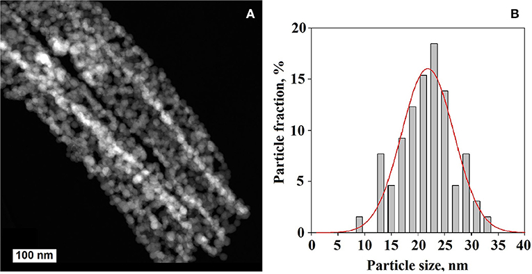
X-ray powder diffraction data indicate that the annealing of zinc hydroxycarbonate results in the formation of ZnO with the wurtzite structure (Supplementary Figure 1). The average crystallite size, calculated from the broadening of the reflections using the Scherrer formula, is 15 ± 2 nm. The specific surface area was estimated from the low-temperature nitrogen adsorption data using the BET model to be 30 ± 5 m2/g. According to the HAADF-STEM images (Figure 1), the material is composed of crystalline ZnO particles of random shape aggregated into agglomerates of mainly rod-shape form. The size of the ZnO particles varies from 8 to 33 nm with an average size of 21 ± 5 nm.
Synthesized CdSe nanocrystals have the crystalline structure of zinc-blende (Supplementary Figure 2). The crystallite size estimated by Scherrer formula is 3.0 ± 0.5 nm. Low magnification TEM images (Figure 2) show that CdSe nanocrystals obtained at 230°C for 35 s are nearly spherical and have a narrow size distribution of 2.8 ± 0.2 nm (Figure 2). The increase in synthesis temperature and duration leads to the growth of CdSe crystals up to 3.3 ± 0.1 nm. As a result of the formation of the CdS shell, the average size of nanocrystals increases to 4.2 ± 0.5 nm while maintaining a narrow size distribution (Figure 2). Thus, the shell thickness is about 0.5 nm, corresponding to ~ 1 monolayer of CdS.
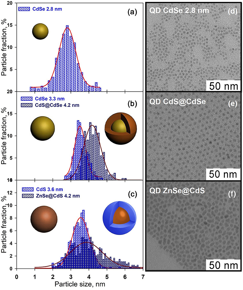
Figure 2. Left panels: Particle size distribution of CdSe (a), CdS@CdSe (b), and ZnSe@CdS (c) nanocrystals. For CdS@CdSe and ZnSe@CdS heterostructures, the size distribution for the CdSe and CdS core is also presented. Right panels: Low magnification TEM images of CdSe (d), CdS@CdSe (e), and ZnSe@CdS (f) nanocrystals.
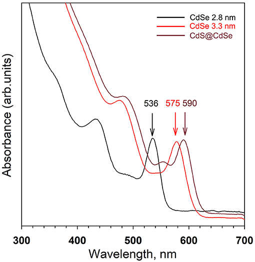
The absorption spectrum of the CdSe nanocrystals has the series of exciton transitions characteristic for spherical quantum dots with the distinct low-energy absorption maximum corresponding to the first exciton transition 1Sh3/2–1Se at λ = 536 nm (Figure 3). The increase in the particle size from 2.8 to 3.3 nm leads to a red shift of this absorption maximum by 40 nm, while maintaining a bandwidth due to narrow dispersion of sizes. The formation of CdS shell on the CdSe nuclei results in a further shift of the exciton maximum to the red region (λ = 590 nm) and retains a sharp exciton band confirming type I heterostructure formation. A small but distinct red shift corresponds to the delocalization of electron over the whole core–shell nanoparticle volume. At the same time, the hole remains localized in the CdSe core, which is supported by a strong increase in luminescence.
The average size of the synthesized CdS nanocrystals determined by TEM was 3.6 ± 0.8 nm. According to X-ray diffraction data, the synthesized CdS nanocrystals have a zinc blende structure (Supplementary Figure 3) and average size 4.0 ± 0.5 nm based on the broadening of the reflections. The buildup of the ZnSe shell on the surface of the CdS nuclei leads to an increase in the average particle size to 4.2 ± 1.2 nm accompanied by a substantial broadening of the particle size distribution (Figure 2). The ZnSe shell thickness thus does not exceed 1 nm, explaining why it is not detected by X-ray diffraction. The reflections of the CdS phase of the ZnSe@CdS heterostructures are shifted toward larger angles (Supplementary Figure 3). This corresponds to a decrease in the interplanar distances, and, consequently, of the unit cell parameter, which may be due to the compression of the CdS nucleus by the ZnSe shell with a smaller unit cell parameter.
The structure of ZnSe@CdS nanocrystals was investigated in detail by high resolution high angle annular dark field scanning transmission electron microscopy (HAADF-STEM) and electron energy loss spectroscopy (EELS). The sample consists of particles with a crystalline core and amorphous shell (Figure 4). The HAADF-STEM image of ZnSe@CdS nanocrystals (Figure 4) reveals the perfect crystal structure of the CdS core with a clear projection of the atomic columns. The corresponding Fast Fourier Transform (FFT) of the selected area (marked in a white square) can be indexed as the zinc-blende structure with a [001] zone axis.
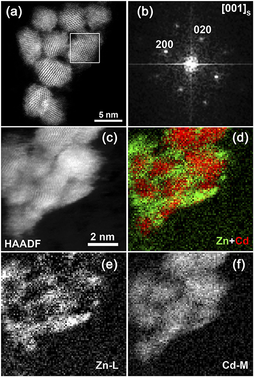
Figure 4. (a,b) HAADF-STEM image of the ZnSe@CdS nanocrystals and Fourier transform of the selected area indexed in the zinc-blende structure; (c–f) HAADF-STEM image of the ZnSe@CdS nanocrystals, the maps of the Zn-L and Cd-M EELS signals and the color-coded mixed compositional map.
The size of the crystalline core varies between 3 and 14 nm with the average value of 6 ± 2 nm. The thickness of the amorphous layer is of 1–2 nm. According to the STEM-EELS compositional mapping, the crystalline core of the particles contains Cd, whereas the amorphous layer around the core contains Zn (Figure 4).
Analysis of the optical properties during the shell growth of ZnSe@CdS nanocrystals was used to verify type II heterostructure formation. The change in the absorption spectra of ZnSe@CdS nanocrystals is shown in Figure 5A as a function of the growth time (0–180 min) of the ZnSe shell on the surface of the CdS nuclei. The first exciton maximum in the 440–460 nm region is observed in the absorption spectrum of the CdS nanocrystals. With increasing ZnSe shell growth time, the band corresponding to an electronic transition in a heterostructure of type II with a spectral position of 550–620 nm can be distinguished in semilogarithmic coordinates (Figure 5A, inset). The profile of the spectra shows the appearance, growth of intensity and shift of this band to the red region. The form of the spectrum in the short-wavelength region remains practically unchanged. The inflection corresponding to the exciton absorption on the spectrum of the original CdS nuclei is conserved on the ZnSe@CdS nanocrystals spectra.
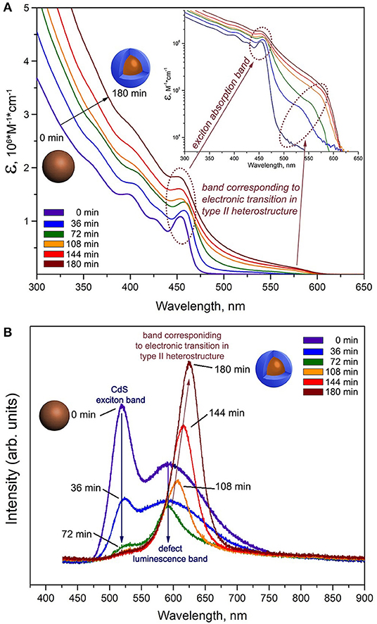
Figure 5. (A) Evolution of optical absorption spectra of aliquots taken from the reaction mixture during the growth of the ZnSe shell on CdS nuclei in function of growth time (0–180 min). The data are presented in the form of spectral dependence of extinction coefficient ε. Inset: Absorption spectra in semilogarithmic coordinates. (B) Evolution of luminescence spectra of aliquots taken from the reaction mixture during the growth of the ZnSe shell on CdS nuclei in function of growth time (0–180 min).
A narrow exciton band (520 nm, 2.38 eV) and a wide defect band in the long-wave region of the spectrum (550–700 nm) are present in the luminescence spectrum of the CdS nanocrystals (Figure 5B). As in the case of the absorption spectra, the change in the luminescence spectra with the growth time of the ZnSe shell proves that the system under investigation belongs to type II heterostructures. The appearance and growth of the intensity of the luminescence band in the long-wave region (600–625 nm) is observed in the luminescence spectra. The energy of this band is less than the band gap of the core material (Eg (CdS) = 2.42 eV, ~ 512 nm) and the shell material (Eg (ZnSe) = 2.82 eV, ~440 nm), confirming the formation of a type II heterostructure (Ivanov et al., 2007). Simultaneously, the luminescence band caused by the recombination of charge carriers on defects disappears practically completely, indicating the passivation of surface defects of CdS.
To determine the effect of nanocrystals of CdSe, CdS@CdSe, and ZnSe@CdS on ZnO electrical properties under visible light illumination, the spectral dependences of the photoconductivity of QD/ZnO (QD = CdSe, CdS@CdSe, ZnSe@CdS) nanocomposites were investigated (Figure 6). The photoconductivity of pure ZnO in these conditions is negligibly small (Chizhov et al., 2014, 2016). The appearance and maxima in the photoresponse curve of the nanocomposites matches well with the onset and the maxima in the absorption spectra of the QDs. For all ZnO/QD nanocomposites, there is an important increase in the photoconductivity in the visible range (λ < 600 nm) under illumination with a photon energy of 2.06 eV which is much less than the ZnO band gap (3.3 eV). This indicates the transfer of electrons, photoexcited at quantum dots, to the conduction band of the semiconductor oxide.
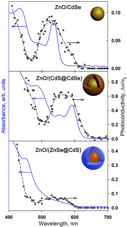
Figure 6. Absorption spectra and spectral dependences of photoconductivity of ZnO/QDs nanocomposites.
Our previous studies of the photoconductivity and gas sensor properties of nanocrystalline ZnO sensitized with CdSe and InP quantum dots have shown that the periodic backlight mode is more convenient than the constant one (Chizhov et al., 2018). This periodic mode consists in alternation of short (2 min) light on/off periods that leads to the corresponding periodic change in photoconductivity. When the lighting cycle is repeated multiple times, the system comes to a stationary state, which can be characterized by the minimum sensor resistance Rλ, which is achieved under illumination, and the maximum sensor resistance Rdark, which is achieved in dark period.
When illuminated with a green LED (λmax = 535 nm), a decrease in the resistance is observed for all nanocomposites (Figure 7, inset). When the light is turned off, the resistance of the nanocomposites increases. Such a change in the electrophysical characteristics of the nanocomposites is due to the simultaneous occurrence of a complex set of processes. When the nanocomposite is illuminated by radiation corresponding to the energy of the first exciton transition 1Sh-1Se, an electron-hole pair is generated in the quantum dot and the electron is excited to the corresponding energy level. The main mechanism for transfer of photoexcitation from quantum dots to metal oxide is the injection (transfer) of charge carriers. From the thermodynamic point of view, the possibility of injecting charge carriers is provided by lowering the free energy of the system because of this process. In the first approximation, one can assume that the condition for the injection of electrons from the quantum dot into the metal oxide is the position of the 1Se level above the bottom of the conduction band (Chizhov et al., 2016). This case is observed in the sensitization of oxides such as In2O3, SnO2, ZnO, with AIIBVI, AIVBVI, AIIIBV quantum dots etc. Electron transfer in the opposite direction—from metal oxide to photoexcited QD is possible if the position of the 1Sh level is below the bottom of the conduction band, which can also be regarded as the injection of holes from the photoexcited QD into the valence band of the metal oxide. This case is less common, and is observed, for example, with the sensitization of NiO with CdSe quantum dots (Zheng et al., 2014). Thus, the preferred direction of photoinduced electron transfer between the metal oxide and the quantum dot is determined by the mutual arrangement of their electronic levels.
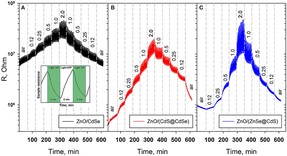
Figure 7. Room temperature electrical resistance of (A) ZnO/CdSe, (B) ZnO/(CdS@CdSe), and (C) ZnO/(ZnSe@CdS) nanocomposites under periodic green light illumination (λmax = 535 nm) depending on NO2 content in the gas phase (in ppm). Inset: change of the sensing layer resistance under periodic LED illumination.
Another process that causes a change in the electrophysical properties of a semiconductor under illumination is the photostimulated desorption of adsorbed molecules. It is known that the interaction of the atmospheric oxygen with the surface of n-type semiconductor oxides leads to the formation of molecular and atomic chemisorbed forms of oxygen. At temperatures below 200°C, the predominant form is molecular ion :
where O2(gas) is an oxygen molecule in the gas phase. The localization of electrons on chemisorbed particles results in the formation of an electron depleted layer near the surface of the semiconductor oxide and in an increase in the resistance of the semiconductor under dark conditions. Under illumination, the photoexcited holes can be transferred from quantum dots to the metal oxide by switching to local energy levels inside its forbidden zone (in other words, the electron is transferred from the local level of metal oxide to the quantum dot, resulting in the recovery of its electroneutrality). The holes transferred in this way can recombine with the electrons localized by chemisorbed oxygen on the surface of a semiconductor oxide:
As a consequence, the oxygen molecule passes into a neutral physically adsorbed form, which can be removed back to the gas phase while the electron trapped by the oxygen returns to the semiconductor. So, the absorption of one photon actually leads to the transfer of two electrons into the conduction band of the metal oxide (Medved, 1961).
The sensor properties in NO2 detection with periodic illumination were measured at room temperature for all nanocomposites. The concentration of NO2 was changed stepwise, first increasing, then decreasing. The duration of each stage was 60 min, so 15 “dark–illumination” cycles were recorded for each NO2 concentration.
As the concentration of NO2 grows, both the resistances Rλ and Rdark increase (Figure 7). Using the example of SnO2, the authors (Sergent et al., 2007) showed by Raman spectroscopy that the electrical conductivity of n-type semiconductor oxides in the presence of NO2 correlates with the concentration of surface bidentate nitrite groups. So, based on the assumption that the chemisorption of NO2 molecules proceeds with the capture of the conduction electron, and the chemisorbed NO2 species are not dissociated, the following processes can be responsible for the formation of sensor response toward NO2:
Due to the significant difference in the electron affinities Eaff of O2 and NO2 molecules (0.45 and 2.27 eV, respectively), the equilibrium (5) is shifted to the right, and chemisorbed NO2 species should form deeper local levels in the forbidden zone of zinc oxide, on which the electrons localize. Therefore, even in the presence of excess of oxygen, the concentration of NO2 in air becomes the controlling factor affecting the semiconductor conductivity.
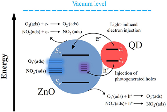
Under green light illumination, when photoexcitation of the quantum dots occurs, the photoexcited electrons are injected from the QD into the oxide matrix, but photoexcited holes remain at the QD. Through interaction with local levels within the forbidden ZnO band, these photoexcited holes can also be injected into the oxide matrix, where they then recombine with the electrons localized in chemisorbed molecules of O2 (Equation 3) and NO2:
The result of this process is the release of an electron captured by chemisorbed molecules, the transition of molecules involved in the recombination into a physically adsorbed form, followed by their desorption, and the recovery of the quantum dot electrical neutrality. A schematic diagram of the interaction between ZnO matrix, QD and NO2 molecules is shown in Figure 8.
The comparison of hybrid materials can be made based on a diagram reflecting the position of the energy bands and levels in the systems under investigation (Figure 9). The positions of ZnO valence (EV) and conduction (EC) bands were taken from Stevanović et al. (2014), and the positions of the 1Sh and 1Se energy levels in CdSe quantum dots and CdS@CdSe and ZnSe@CdS heterostructures were calculated from optical absorption spectra. For this calculation we assumed that on decreasing size of the nanocrystals, the displacement of the edges of the valence and conduction bands is inversely proportional to the effective mass of electrons and holes in this material (Klimov, 2000; Vasiliev et al., 2011). In the model we propose, the most uncertain information is the energy of electrons localized in chemisorbed O2 and NO2 molecules. The literature states that the levels of electrons in O2 molecules chemisorbed on the ZnO surface are 1.1–0.8 eV below the edge of the conduction band (Kiselev and Krylov, 2012). The information on the energy of trapped electrons in chemisorbed NO2 molecules is not available. However, since for ZnO/CdSe nanocomposites the total recovery of conductivity to the base value occurs in experiments with NO2 under constant illumination (Chizhov et al., 2014) it can be assumed that this is due to the complete NO2 photodesorption. This is the case when the local levels of trapped electrons in the chemisorbed NO2 molecules are close in energy with the 1Sh energy level in QDs. From the diagram in Figure 9 one can see that in such case the assumed position of the electron levels in can be in the range of 1.2–2.3 eV below the edge of the ZnO conduction band.
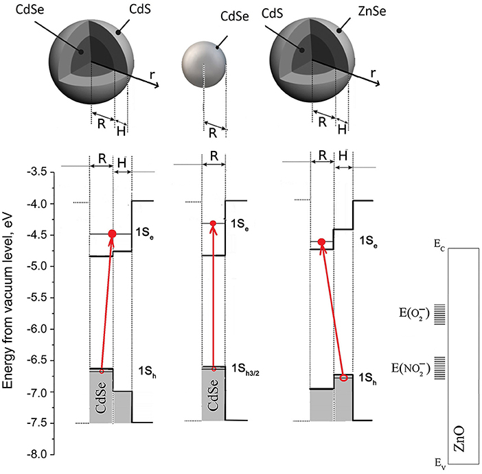
Figure 9. Band diagram for ZnO/CdSe, ZnO/(CdS@CdSe), and ZnO/(ZnSe@CdS) systems. Band alignment for core-shell nanocrystals with core radius R and shell thickness H is shown. Band parameters are taken from O'Connor et al. (2012) and Yang et al. (2014). Electron-hole separation is shown by red arrows.
When performing gas sensor measurements under periodic illumination conditions, the sensor signal may be calculated in different ways: (i) as the ratio of dark resistances S = Rdark/Rdark0, where Rdark is the dark resistance at given NO2 concentration, Rdark0 is the dark resistance in pure air; (ii) as the amplitude of effective photoresponse Peff = Rdark/Rλ at given NO2 concentration. The change of these parameters with increasing and decreasing NO2 concentration in air is presented in Figure 10. For nanocomposites ZnO/CdSe and ZnO/(CdS@CdSe) the concentration dependencies of the sensor signal are linear in double logarithmic coordinates (Figure 10A) that indicates their power-law nature, typical for the resistive type sensors (Yamazoe and Shimanoe, 2008):
Approximation of the experimental dependencies (with increasing NO2 concentration) by the power function gives m = 0.5 and m = 1 for ZnO/CdSe and ZnO/(CdS@CdSe), respectively. For the latter system, perfect passivation of the CdSe core defect states eliminates side effects (Drozdov et al., 2013). This ensures the maximum concentration of electrons photogenerated at the quantum dot and transferred to the conduction band of the semiconductor during illumination, which can be then captured in dark conditions by the acceptor NO2 molecules in accordance with the reaction (4). The concentration dependence of the sensor signal of nanocomposite ZnO/(ZnSe@CdS) is not linearized in double logarithmic coordinates. This dissimilarity may be caused by the fact that the shell growth on the core nanocrystal results in formation of heterostructures with different electron-hole spatial localization. In CdS@CdSe nanocrystals the photogenerated hole is localized strongly inside CdSe core, whereas the photoexcited electron is delocalized over whole core/shell nanocrystal. Oppositely, in ZnSe@CdS nanocrystals the electron is localized inside CdS core, whereas the hole is localized inside ZnSe shell.
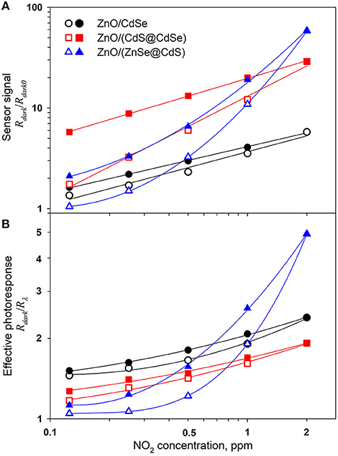
Figure 10. Sensor signal S = Rdark/Rdark0 (A) and effective photoresponse Peff = Rdark/Rλ (B) of ZnO/CdSe, ZnO/(CdS@CdSe), and ZnO/(ZnSe@CdS) nanocomposites under periodic green light illumination (λmax = 535 nm) with increasing (open symbols) and decreasing (filled symbols) NO2 concentration in the gas phase.
As can be seen from the energy diagram (Figure 9), the formation of ZnSe@CdS type II heterostructure does not lead to a drastic change in the position of the 1Sh and 1Se levels of a hole and an electron, respectively, as compared with a CdSe quantum dot and CdS@CdSe type I heterostructure. At the same time, the probability of the electron and hole transfer processes between the sensitizer and ZnO matrix is fundamentally different. The preferential spatial localization of a hole in the ZnSe shell (Ivanov et al., 2007) provides its more efficient transfer from the ZnSe@CdS sensitizer to the ZnO matrix. This leads to an increase in the probability of tunneling of electrons localized at the acceptor levels of chemisorbed NO2 molecules to the 1Sh level at the sensitizer, promoting NO2 desorption. In other words, in a quasi-equilibrium state under photoexcitation conditions, the larger efficiency of hole transfer from the ZnSe shell to localized levels in the ZnO forbidden band as compared with electron transfer from the CdS nucleus to the ZnO conduction band will lead to the partial negative charging of ZnSe@CdS nanocrystals. This, in turn, will lead to the discharge of the acceptor levels in the ZnO band gap, corresponding to the electrons trapped by chemisorbed NO2 molecules.
Thus, in ZnSe@CdS nanocrystals, the shell plays a dual role. On the one hand, as in the case of type I heterostructure CdS@CdSe, the shell formation leads to the perfect passivation of CdS core defect states, ensuring the maximum concentration of photogenerated electrons transferred to the ZnO conduction band and then captured by the acceptor NO2 molecules in dark interval of the measurement cycle. On the other hand, the localization of a hole in ZnSe shell ensures the efficient charge transfer from chemisorbed NO2 molecules and their subsequent desorption in the light interval of the measurement cycle. The synergetic combination of these factors leads to a significant increase in the light activated sensor sensitivity to NO2 in case of ZnO/ZnSe@CdS nanocomposites compared with ZnO/CdSe and ZnO/(CdS@CdSe) samples.
The validity of these arguments is confirmed by the character of the NO2 concentration dependence of the effective photoresponse for different nanocomposites (Figure 10B). The hole localization in the CdSe core reduces the efficiency of its transfer to the ZnO matrix that leads to a decrease in the photoresponse of the ZnO/(CdS@CdSe) nanocomposite in comparison with ZnO/CdSe. On the contrary, the hole localization in the ZnSe shell promotes the transfer of electrons from acceptor levels in the ZnO forbidden zone. Consequently, the effective photoresponse of ZnO/(ZnSe@CdS) nanocomposite grows rapidly with increasing NO2 concentration in air.
At the same time, as one can note from Figure 7, the sensors containing CdS@CdSe and ZnSe@CdS core-shell nanoparticles exhibit significant signal drift. The reasons of this drift can be discussed as follows. Formation of the type I CdS(shell)@CdSe(core) heterostructure with a straddling gap arrangement leads to the perfect passivation of CdSe core defect states and to the localization of photogenerated holes inside the CdSe core. The first factor determines the increase in sensor sensitivity toward NO2, while the latter one leads to the decrease in effective photoresponse at given NO2 concentration, and increase in the time needed to recover the signal of ZnO/(CdS@CdSe) nanocomposites as compared with ZnO/CdS hybrid material. In ZnO/(ZnSe@CdS) hybrid material the hole localization in the shell of nanoparticle CdS@CdSe results in the increase of contribution from the capturing of photoexcited charges at surface traps. This changes the charge-injection processes at the nanocrystal-matrix interface. It may lead to long-lived charge accumulation and the increase of the relaxation time resulted in the change of steady-state conductivity.
The effect of humidity on the values of the sensor response and the effective photoresponse as a function of the NO2 concentration was studied for ZnO/CdSe hybrid materials. Figure 11 shows the change in room temperature electrical resistance of ZnO/CdSe nanocomposites under periodic green light illumination depending on NO2 content in dry (RH25 = 0%) and humid (RH25 = 20% and RH25 = 40%) air. We have to note the following: with increasing humidity, (i) the resistance of ZnO/CdSe in pure air decreases, and (ii) the sensor response and the effective photoresponse of ZnO/CdSe increase. This may be due to the adsorption of water vapor on the ZnO surface, which leads to an increase in the concentration of free charge carriers (electrons) in n-type semiconductor oxides (Bârsan and Weimar, 2001). In turn, this stimulates the adsorption of NO2 by reaction (4), which leads to an increase in the sensor signal and an increase in the effective photoresponse (Figure 12). The low detection limit (LDL) values were calculated from the calibration curves as NO2 concentration corresponding to the minimum measurable sensor signal (Rav + 3σ)/Rav, where Rav is the average dark resistance in pure air with given humidity, σ is the standard deviation of average dark resistance in pure air with given humidity. An increase in the air humidity is accompanied by a decrease in LDL from 58 ppb (RH25 = 0%) to 49 ppb (RH25 = 40%).
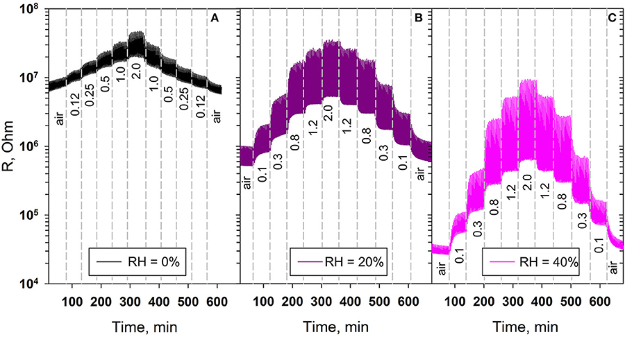
Figure 11. Room temperature electrical resistance of ZnO/CdSe nanocomposites under periodic green light illumination (λmax = 535 nm) depending on NO2 content in the gas phase (in ppm) at (A) RH25 = 0%, (B) RH25 = 20%, (C) RH25 = 40%.
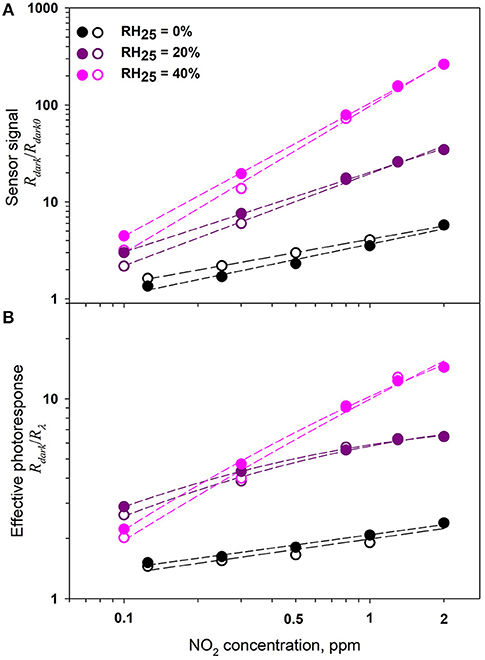
Figure 12. Sensor signal S = Rdark/Rdark0 (A) and effective photoresponse Peff = Rdark/Rλ (B) of ZnO/CdSe nanocomposite under periodic green light illumination (λmax = 535 nm) with increasing (open symbols) and decreasing (filled symbols) NO2 concentration in the gas phase at different humidity.
Conclusions
We investigated the photoconductivity and visible light activated room temperature NO2 gas sensor properties of hybrid materials based on nanocrystalline ZnO sensitized with two types of core/shell nanoparticles with different localization of photoexcited electron-hole pair between the core and the shell. Formation of the type I CdS(shell)@CdSe(core) heterostructure with a straddling gap arrangement leads to the localization of photogenerated holes inside the CdSe core and to the perfect passivation of CdSe core defect states. These factors determine the increase of sensor sensitivity toward NO2 and the decrease of effective photoresponse at given NO2 concentration of ZnO/(CdS@CdSe) nanocomposites as compared with ZnO/CdS hybrid material. In type II ZnSe(shell)@CdS(core) heterostructures with staggered gap, the shell formation also provides the perfect passivation of CdS core defect states but in this case the photogenerated hole localization in the ZnSe shell ensures the efficient charge transfer from chemisorbed NO2 molecules and their subsequent desorption under illumination. Compared with ZnO/CdSe and ZnO/(CdS@CdSe) samples, in case of ZnO/ZnSe@CdS nanocomposites the synergetic combination of these factors leads to a significant increase in the light activated sensor sensitivity to NO2 and to the rapid growth of effective photoresponse with increasing NO2 concentration in air.
Thus, the use of heterostructures with different spatial separation of photogenerated charges opens new possibilities in controlling the photoelectric and light activated gas sensor properties of hybrid nanomaterials based on wide gap semiconductor oxides with quantum dots of narrow-band semiconductors as photosensitizers.
Data Availability Statement
All datasets generated for this study are included in the manuscript/Supplementary Files.
Author Contributions
AC, RV, MR, and AG contributed conception and design of the study. AC and RV performed the synthesis of all the materials. RV effectuated the optical characterization of the materials. AC performed the sensor measurements. IK and KD conducted photoelectrical characterization of the materials. MB, JH, and AA effectuated HAADF-STEM and EELS analysis. MR and RV wrote the first draft of the manuscript. All authors contributed to manuscript revision, read, and approved the submitted version.
Funding
This work was financially supported by RFBR grant No. 16-53-76001 (RFBR – ERA.Net FONSENS 096) and in part by a grant from the St. Petersburg State University – Event 3-2018 (id: 26520408). AC acknowledges support from the RFBR grant No. 18-33-01004.
Conflict of Interest
The authors declare that the research was conducted in the absence of any commercial or financial relationships that could be construed as a potential conflict of interest.
Supplementary Material
The Supplementary Material for this article can be found online at: https://www.frontiersin.org/articles/10.3389/fmats.2019.00231/full#supplementary-material
References
Bârsan, N., and Weimar, U. (2001). Conduction model of metal oxide gas sensors. J. Electroceram. 7, 143–167. doi: 10.1023/A:1014405811371
Carotta, M. C., Cervi, A., Fioravanti, A., Gherardi, S., Giberti, A., Vendemiati, B., et al. (2011). A novel ozone detection at room temperature through UV-LED-assisted ZnO thick film sensors. Thin Solid Films 520, 939–946. doi: 10.1016/j.tsf.2011.04.173
Chizhov, A., Rumyantseva, M., Vasiliev, R., Filatova, D., Drozdov, K., Krylov, I., et al. (2016). Visible light activation of room temperature NO2 gas sensors based on ZnO, SnO2 and In2O3 sensitized with CdSe quantum dots. Thin Solid Films 618, 253–262. doi: 10.1016/j.tsf.2016.09.029
Chizhov, A. S., Mordvinova, N. E., Rumyantseva, M. N., Krylov, I. V., Drozdov, K. A., Li, X., et al. (2018). The effect of CdSe and InP quantum dots on the interaction of ZnO with NO2 under visible light irradiation. Russ. J. Inorg. Chem. 63, 512–518. doi: 10.1134/S0036023618040071
Chizhov, A. S., Rumyantseva, M. N., Vasiliev, R. B., Filatova, D. G., Drozdov, K. A., Krylov, I. V., et al. (2014). Visible light activated room temperature gas sensors based on nanocrystalline ZnO sensitized with CdSe quantum dots. Sens. Actuators B 205, 305–312. doi: 10.1016/j.snb.2014.08.091
Cui, J., Wang, D., Xie, T., and Lin, Y. (2013). Study on photoelectric gas-sensing property and photogenerated carrier behavior of Ag–ZnO at the room temperature. Sens. Actuators B 186, 165–171. doi: 10.1016/j.snb.2013.05.088
Da Silva, L. F., M'Peko, J.-C., Catto, A. C., Bernardini, S., Mastelaro, V. R., Aguir, K., et al. (2017). UV-enhanced ozone gas sensing response of ZnO-SnO2 heterojunctions at room temperature. Sens. Actuators B 240, 573–579. doi: 10.1016/j.snb.2016.08.158
De Lacy Costello, B. P. J., Ewen, R. J., Ratcliffe, N. M., and Richards, M. (2008). Highly sensitive room temperature sensors based on the UV-LED activation of zinc oxide nanoparticles. Sens. Actuators B 134, 945–952. doi: 10.1016/j.snb.2008.06.055
Drozdov, K. A., Kochnev, V. I., Dobrovolsky, A. A., Popelo, A. V., Rumyantseva, M. N., Gaskov, A. M., et al. (2013). Photoconductivity of structures based on the SnO2 porous matrix coupled with core-shell CdSe/CdS quantum dots. Appl. Phys. Lett. 103:133115. doi: 10.1063/1.4823549
Espid, E., and Taghipour, F. (2017). UV-LED photo-activated chemical gas sensors: a review. Crit. Rev. Solid State Mater. Sci. 42, 416–432. doi: 10.1080/10408436.2016.1226161
Geng, Q., He, Z., Chen, X., Dai, W., and Wang, X. (2013). Gas sensing property of ZnO under visible light irradiation at room temperature. Sens. Actuators B 188, 293–297. doi: 10.1016/j.snb.2013.07.001
Geng, X., You, J., and Zhang, C. (2016a). Microstructure and sensing properties of CdS-ZnO1−x coatings deposited by liquid plasma spray and treated with hydrogen peroxide solution for nitrogen dioxide detection at room temperature. J. Alloys Compd. 687, 286–293. doi: 10.1016/j.jallcom.2016.06.079
Geng, X., Zhang, C., and Debliquy, M. (2016b). Cadmium sulfide activated zinc oxide coatings deposited by liquid plasma spray for room temperature nitrogen dioxide detection under visible light illumination. Ceram. Int. 42, 4845–4852. doi: 10.1016/j.ceramint.2015.11.170
Han, L., Wang, D., Cui, J., Chen, L., Jiang, T., and Lin, Y. (2012). Study on formaldehyde gas-sensing of In2O3-sensitized ZnO nanoflowers under visible light irradiation at room temperature. J. Mater. Chem. 22, 1295–12920. doi: 10.1039/c2jm16105b
Han, L., Wang, D., Lu, Y., Jiang, T., Chen, L., Xie, T., et al. (2013). Influence of annealing temperature on the photoelectric gas sensing of Fe-doped ZnO under visible light irradiation. Sens. Actuators B 177, 34–40. doi: 10.1016/j.snb.2012.10.096
Hsu, C.-L., Chang, L.-F., and Hsueh, T.-J. (2017). Light-activated humidity and gas sensing by ZnO nanowires grown on LED at room temperature. Sens. Actuators B 249, 265–277. doi: 10.1016/j.snb.2017.04.083
Hyodo, T., Urata, K., Kamada, K., Ueda, T., and Shimizu, Y. (2017). Semiconductor-type SnO2-based NO2 sensors operated at room temperature under UV-light irradiation. Sens. Actuators B 253, 630–640. doi: 10.1016/j.snb.2017.06.155
Ilin, A., Martyshov, M., Forsh, E., Forsh, P., Rumyantseva, M., Abakumov, A., et al. (2016). UV effect on NO2 sensing properties of nanocrystalline In2O3. Sens. Actuators B 231, 491–496. doi: 10.1016/j.snb.2016.03.051
Ivanov, S. A., Piryatinski, A., Nanda, J., Tretiak, S., Zavadil, K. R., Wallace, W. O., et al. (2007). Type-II core/shell CdS/ZnSe nanocrystals: synthesis, electronic structures, and spectroscopic properties. J. Am. Chem. Soc. 129, 11708–11719. doi: 10.1021/ja068351m
Kim, Y.-S., Hummer, K., and Kresse, G. (2009). Accurate band structures and effective masses for InP, InAs, and InSb using hybrid functionals. Phys. Rev. B 80:035203. doi: 10.1103/PhysRevB.80.035203
Kiselev, V. F., and Krylov, O. V. (2012). “Adsorption and catalysis on transition metals,” in Adsorption and Catalysis on Transition Metals and Their Oxides (Springer Series in Surface Sciences), Vol. 9, eds G. Ertl, R. Gomer, and H. K. V. Lotsch (Berlin; Heidelberg: Springer; Springer Science + Business Media), 136–265.
Klaus, D., Klawinski, D., Amrehn, S., Tiemann, M., and Wagner, T. (2015). Light-activated resistive ozone sensing at room temperature utilizing nanoporous In2O3 particles: influence of particle size, Sens. Actuators B 217, 181–185. doi: 10.1016/j.snb.2014.09.021
Klimov, V. I. (2000). Optical nonlinearities and ultrafast carrier dynamics in semiconductor nanocrystals. J. Phys. Chem. B 104, 6112–6123. doi: 10.1021/jp9944132
Krivetskiy, V. V., Rumyantseva, M. N., and Gaskov, A. M. (2013). Chemical modification of nanocrystalline tin dioxide for selective gas sensors. Russ. Chem. Rev. 82, 917–941. doi: 10.1070/RC2013v082n10ABEH004366
Malagu, C., Carotta, M. C., Comini, E., Faglia, G., Giberti, A., Guidi, V., et al. (2005). Photo-induced unpinning of Fermi level in WO3. Sensors 5, 594–603. doi: 10.3390/s5120594
Medved, D. (1961). Photoconductivity and chemisorption kinetics in sintered zinc oxide semiconductor. J. Phys. Chem. Solids 20, 255–267. doi: 10.1016/0022-3697(61)90012-9
Minami, T., Miyata, T., and Yamamoto, T. (1998). Work function of transparent conducting multicomponent oxide thin films prepared by magnetron sputtering. Surf. Coat. Technol. 108–109, 583–587. doi: 10.1016/S0257-8972(98)00592-1
Mishra, S., Ghanshyam, C., Ram, N., Bajpai, R. P., and Bedi, R. K. (2004). Detection mechanism of metal oxide gas sensor under UV radiation. Sens. Actuators B 97, 387–390. doi: 10.1016/j.snb.2003.09.017
Mordvinova, N. E., Vinokurov, A. A., Dorofeev, S. G., Kuznetsova, T. A., and Znamenkov, K. O. (2014). Phosphine synthetic route features and post synthetic treatment of InP quantum dots. J. Alloys Compd. 582, 43–49. doi: 10.1016/j.jallcom.2013.08.003
Nakate, U. T., Patil, P., Bulakhe, R. N., Lokhande, C. D., Kale, S. N., Naushad, M., et al. (2016). Sprayed zinc oxide films: ultra-violet light-induced reversible surface wettability and platinum-sensitization-assisted improved liquefied petroleum gas response. J. Colloid Interface Sci. 480, 109–117. doi: 10.1016/j.jcis.2016.07.010
O'Connor, T., Panov, M. S., Mereshchenko, A., Tarnovsky, A. N., Lorek, R., Perera, D., et al. (2012). The effect of the charge-separating interface on exciton dynamics in photocatalytic colloidal heteronanocrystals. ACS Nano 6, 8156–8165. doi: 10.1021/nn302810y
Paolesse, R., Nardis, S., Monti, D., Stefanelli, M., and Di Natale, C. (2017). Porphyrinoids for chemical sensor applications. Chem. Rev. 117, 2517–2583. doi: 10.1021/acs.chemrev.6b00361
Peng, L., Qin, P., Zeng, Q., Song, H., Lei, M., Mwangi, J. J. N., et al. (2011). Improvement of formaldehyde sensitivity of ZnO nanorods by modifying with Ru(dcbpy)2(NCS)2. Sens. Actuators B 160, 39–45. doi: 10.1016/j.snb.2011.07.008
Peng, L., Xie, T., Yang, M., Wang, P., Xu, D., Pang, S., et al. (2008). Light induced enhancing gas sensitivity of copper-doped zinc oxide at room temperature. Sens. Actuators B 131, 660–664. doi: 10.1016/j.snb.2007.12.060
Peng, L., Zhao, Q., Wang, D., Zhai, J., Wang, P., Pang, S., et al. (2009). Ultraviolet-assisted gas sensing: a potential formaldehyde detection approach at room temperature based on zinc oxide nanorods. Sens. Actuators B 136, 80–85. doi: 10.1016/j.snb.2008.10.057
Prades, J. D., Diaz, R. J., Hernandez-Ramirez, F., Barth, S., Cirera, A., Romano-Rodriguez, A., et al. (2009a). Equivalence between thermal and room temperature UV light modulated responses of gas sensors based on individual SnO2 nanowires. Sens. Actuators B 140, 337–341. doi: 10.1016/j.snb.2009.04.070
Prades, J. D., Jimenez-Diaz, P., Manzanares, M., Hernandez-Ramirez, F., Cirera, A., Romano-Rodriguez, A., et al. (2009b). A model for the response towards oxidizing gases of photoactivated sensors based on individual SnO2 nanowires. Phys. Chem. Chem. Phys. 11, 10881–10889. doi: 10.1039/b915646a
Rumyantseva, M., Nasriddinov, A., Vladimirova, S., Tokarev, S., Fedorova, O., Krylov, I., et al. (2018). Photosensitive organic-inorganic hybrid materials for room temperature gas sensor applications. Nanomaterials 8:671. doi: 10.3390/nano8090671
Saboor, F. H., Ueda, T., Kamada, K., Hyodo, T., Mortazavi, V., Khodadadi, A. A., et al. (2016). Enhanced NO2 gas sensing performance of bare and Pd-loaded SnO2 thick film sensors under UV-light irradiation at room temperature. Sens. Actuators B 223, 429–439. doi: 10.1016/j.snb.2015.09.075
Saura, J. (1994). Gas-sensing properties of SnO2 pyrolytic films subjected to ultraviolet radiation. Sens. Actuators B 17, 211–214. doi: 10.1016/0925-4005(93)00874-X
Sergent, N., Epifani, M., Comini, E., Faglia, G., and Pagnier, T. (2007). Interactions of nanocrystalline tin oxide powder with NO2: a Raman spectroscopic study. Sens. Actuators B 126, 1–5. doi: 10.1016/j.snb.2006.10.013
Stevanović, V., Lany, S., Ginley, D. S., Tumas, W., and Zunge, A. (2014). Assessing capability of semiconductors to split water using ionization potentials and electron affinities only. Phys. Chem. Chem. Phys. 16, 3706–3714. doi: 10.1039/c3cp54589j
Sun, Z., Huang, D., Yang, Z., Li, X., Hu, N., Yang, C., et al. (2015). ZnO nanowire-reduced graphene oxide hybrids based portable NH3 gas sensing electron device. IEEE Electron Device Lett. 36, 1376–1379. doi: 10.1109/LED.2015.2496177
Trawka, M., Smulko, J., Hasse, L., Granqvist, C.-G., Annanouch, F. E., and Ionescu, R. (2016). Fluctuation enhanced gas sensing with WO3-based nanoparticle gas sensors modulated by UV light at selected wavelengths. Sens. Actuators B 234, 453–461. doi: 10.1016/j.snb.2016.05.032
Varechkina, E. N., Rumyantseva, M. N., Vasiliev, R. B., Konstantinova, E. A., and Gaskov, A. M. (2012). UV-VIS photoconductivity of nanocrystalline tin oxide. J. Nanoelectron. Optoelectron. 7, 1–6. doi: 10.1166/jno.2012.1399
Vasiliev, R., Babynina, A., Maslova, O., Rumyantseva, M., Ryabova, L., Dobrovolsky, A., et al. (2013). Photoconductivity of nanocrystalline SnO2 sensitized with colloidal CdSe quantum dots. J. Mater. Chem.? 1, 1005–1010. doi: 10.1039/C2TC00236A
Vasiliev, R. B., Dirin, D. N., and Gaskov, A. M. (2011). Semiconductor nanoparticles with spatial separation of charge carriers: synthesis and optical properties. Russ. Chem. Rev. 80, 1139–1158. doi: 10.1070/RC2011v080n12ABEH004240
Vorobyeva, N., Rumyantseva, M., Filatova, D., Konstantinova, E., Grishina, D., Abakumov, A., et al. (2013). Nanocrystalline ZnO(Ga): paramagnetic centers, surface acidity and gas sensor properties. Sens. Actuators B 182, 555–564. doi: 10.1016/j.snb.2013.03.068
Wagner, T., Kohl, C.-D., Malagù, C., Donato, N., Latino, M., Neri, G., et al. (2013). UV light-enhanced NO2 sensing by mesoporous In2O3: interpretation of results by a new sensing model. Sens. Actuators B 187, 488–494. doi: 10.1016/j.snb.2013.02.025
Wang, C. Y., Becker, R. W., Passow, T., Pletsche, W., Kohler, K., Cimalla, V., et al. (2011). Photon-stimulated sensor based on indium oxide nanoparticles I: wide-concentration-range ozone monitoring in air. Sens. Actuators B 152, 235–240. doi: 10.1016/j.snb.2010.12.014
Wang, T., Sun, Z., Huang, D., Yang, Z., Ji, Q., Hu, N., et al. (2017). Studies on NH3 gas sensing by zinc oxide nanowire-reduced graphene oxide nanocomposites. Sens. Actuators B 252, 284–294. doi: 10.1016/j.snb.2017.05.162
Wang, T., Xu, S., Hu, N., Hu, J., Huang, D., Jiang, W., et al. (2018). Microwave preparation and remarkable ethanol sensing properties of ZnO particles with controlled morphologies in water-ethylene glycol binary solvent system. Sens. Actuators B 252, 1006–1014. doi: 10.1016/j.snb.2017.08.099
Wongrat, E., Chanlek, N., Chueaiarrom, C., Samransuksamer, B., Hongsith, N., and Choopun, S. (2016). Low temperature ethanol response enhancement of ZnO nanostructures sensor decorated with gold nanoparticles exposed to UV illumination. Sens. Actuators A 251, 188–197. doi: 10.1016/j.sna.2016.10.022
Wu, T., Wang, Z., Tian, M., Miao, J., Zhang, H., and Sun, J. (2018). UV excitation NO2 gas sensor sensitized by ZnO quantum dots at room temperature. Sens. Actuators B 259, 526–531. doi: 10.1016/j.snb.2017.12.101
Xu, F., and Ho, H.-P. (2017). Light-activated metal oxide gas sensors: a review. Micromachines 8, 333. doi: 10.3390/mi8110333
Yamazoe, N., and Shimanoe, K. (2008). Theory of power laws for semiconductor gas sensors. Sens. Actuators B 128, 566–573. doi: 10.1016/j.snb.2007.07.036
Yang, Z., Guo, L., Zu, B., Guo, Y., Xu, T., and Dou, X. (2014). CdS/ZnO core/shell nanowire-built films for enhanced photodetecting and optoelectronic gas-sensing applications. Adv. Opt. Mater. 2, 738–745. doi: 10.1002/adom.201400086
Zhang, C., Geng, X., Li, J., Luo, Y., and Lu, P. (2017). Role of oxygen vacancy in tuning of optical, electrical and NO2 sensing properties of ZnO1−x coatings at room temperature. Sens. Actuators B 248, 886–893. doi: 10.1016/j.snb.2017.01.105
Zhang, C., Wang, J., Olivier, M.-G., and Debliquy, M. (2015). Room temperature nitrogen dioxide sensors based on N719-dye sensitized amorphous zinc oxide sensors performed under visible-light illumination. Sens. Actuators B 209, 69–77. doi: 10.1016/j.snb.2014.11.090
Zheng, K., Žídek, K., Abdellah, M., Zhang, W., Chábera, P., Lenngren, N., et al. (2014). Ultrafast charge transfer from CdSe quantum dots to p-type NiO: hole injection vs hole trapping. J. Phys. Chem. C 118, 18462–18471. doi: 10.1021/jp506963q
Keywords: room temperature semiconductor gas sensor, sub-ppm NO2 detection, visible light activation, CdSe quantum dots, core/shell heterostructures, charge spatial localization
Citation: Chizhov A, Vasiliev R, Rumyantseva M, Krylov I, Drozdov K, Batuk M, Hadermann J, Abakumov A and Gaskov A (2019) Light-Activated Sub-ppm NO2 Detection by Hybrid ZnO/QD Nanomaterials vs. Charge Localization in Core-Shell QD. Front. Mater. 6:231. doi: 10.3389/fmats.2019.00231
Received: 07 May 2019; Accepted: 05 September 2019;
Published: 24 September 2019.
Edited by:
Qasem Ahmed Drmosh, King Fahd University of Petroleum and Minerals, Saudi ArabiaCopyright © 2019 Chizhov, Vasiliev, Rumyantseva, Krylov, Drozdov, Batuk, Hadermann, Abakumov and Gaskov. This is an open-access article distributed under the terms of the Creative Commons Attribution License (CC BY). The use, distribution or reproduction in other forums is permitted, provided the original author(s) and the copyright owner(s) are credited and that the original publication in this journal is cited, in accordance with accepted academic practice. No use, distribution or reproduction is permitted which does not comply with these terms.
*Correspondence: Marina Rumyantseva, cm91bUBpbm9yZy5jaGVtLm1zdS5ydQ==
 Artem Chizhov1
 Marina Rumyantseva
 Ivan Krylov
 Joke Hadermann
 Alexander Gaskov