 Wenjun Chen
 Oscar Vazquez-Mena
- Department of Nano Engineering, Center for Memory and Recording Research, Calibaja Center for Resilient Materials and Systems, University of California, San Diego, La Jolla, CA, United States
Colloidal quantum dots (QDs) are of great interest in optoelectronic and photovoltaic devices with low-cost processing, strong light absorption, and size tunable direct band gap. However, their limited carrier mobility and short diffusion length limit efficient charge collection and transport. The short diffusion length in QD solid films, 100–200 nm, limits their thickness to t≈200–300 nm, resulting in poor absorption in the near-infrared, λ>800 nm, wasting part of sunlight and reducing power conversion efficiency. Recently, a novel architecture based on multiple graphene monolayers (Gr) intercalated inside QD films was reported to improve charge extraction beyond QDs diffusion length. The intercalated graphene layers ensure efficient charge collected in QD films thicker than the diffusion length. However, this architecture still fails to collect carriers from the QDs when the thickness is >~200 nm due to the poor vertical conductivity of the devices. Herein, we present the fabrication, optimization, and implementation of intercalated devices with vertical interconnecting contacts, increasing carrier collection, and photocurrent, aiming to develop a novel architecture for improved photodetection and photovoltaics with QDs. First, we analyze the individual roles of Gr and QDs, studying the evolution of light absorption, photocurrent (Iph), and conductivity as successive QD and Gr layers are added. We find the optimal interspacing between graphene layers in the intercalated system, aiming for the best compromise between light absorption and efficient charge collection. Our main contribution is the implementation of vertical interconnect access (VIAs) to each graphene layer to ensuring efficient charge transfer from Gr to the gold electrical contacts for efficient current collection. We show that for 850 nm wavelength illumination, photocurrent of intercalated devices show a ~10 fold improvement over devices without VIAs. We also use a back-gate voltage to monitor Fermi level shift in Gr and charge transfer from QDs to Gr. The intercalated configuration with VIAs contacts herein presented is a significant improvement in charge collection for QD optoelectronic applications as well as a promising architecture to enhance the power conversion efficiency for QD solar cells.
Efficient charge collection and transport is critical for optoelectronic devices. Despite its low-cost processing, strong light absorption, and size tunable direct band gap, quantum dots (QDs) have poor mobility, limiting its charge collection, and its overall performance in optoelectronic devices and power conversion efficiency (Clifford et al., 2009; Konstantatos and Sargent, 2010; Tang and Sargent, 2011; Sargent, 2012; Lan et al., 2014; Saran and Curry, 2016). Charge carrier transport in solid films of QDs occurs from dot to dot by hopping across surface organic ligands (van der Wiel et al., 2002; Kagan and Murray, 2015). In order to overcome this restriction, recently graphene has been added as efficient charge collection and transporting layer as shown in Figure 1A, resulting in significant improvements on photoresponsivity and film conductivity (Konstantatos et al., 2012; Sun et al., 2012; Kufer et al., 2015; Nikitskiy et al., 2016). Since the charge carrier mobility of graphene (Gr) (~103 cm2V−1s−1) (Koppens et al., 2014; Huo and Konstantatos, 2018) is far superior than for PbS QDs (~10−3 cm2V−1s−1) (Johnston et al., 2008; Katsiev et al., 2014), the carrier transport is greatly enhanced. A further enhancement was achieved by adding intercalated graphene layers instead of a single bottom graphene layer as shown in Figure 1B, adding more conducting channels and facilitating the collection of photocarriers (Chen et al., 2019). Charge carriers in QDs can reach a nearby graphene much easier in intercalated devices than in bottom devices, improving quantum efficiency, and photoresponsivity.
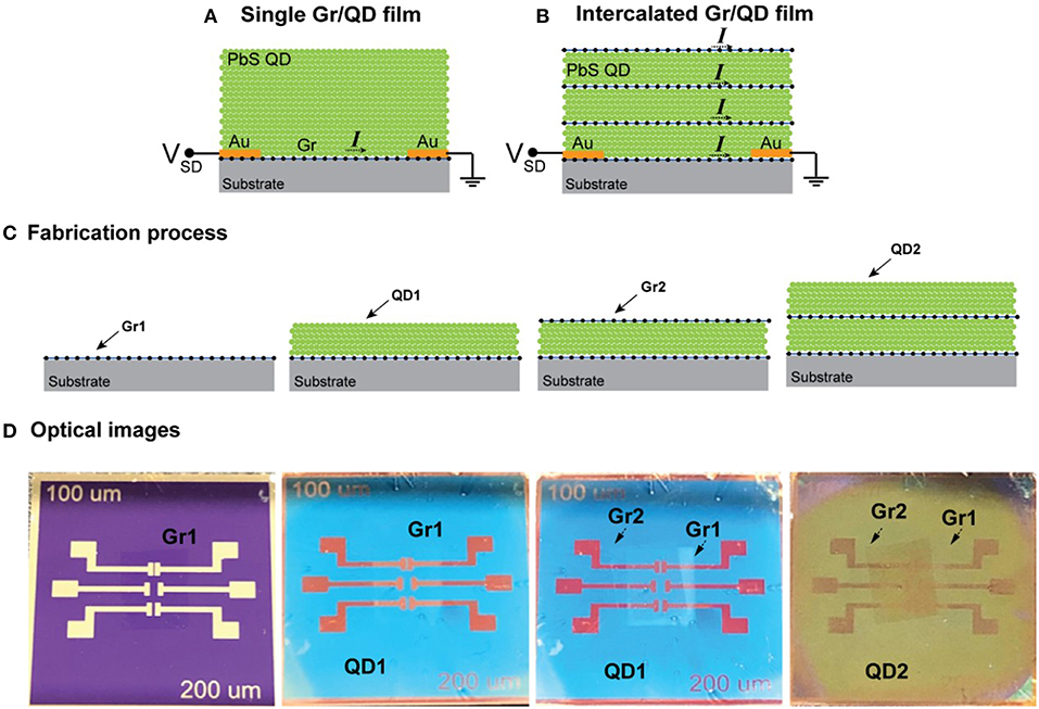
Figure 1. Intercalated devices. (A) Conventional hybrid Gr/QD dot device with single graphene layer at the bottom. (B) Intercalated graphene layers in an intercalated Gr/QDs configuration enhancing charge collection and transport. (C) Schematic of the sequential deposition of Gr and QD layers to realize intercalated devices. (D) Optical images of an intercalated device at each step during fabrication process.
Herein, we analyze individually the role that Gr and QDs play both in the charge transport and in the collection of photogenerated carriers. We study the evolution of light absorption, photocurrent (Iph), and conductivity in intercalated film as successive QD and Gr layers are added, allowing to pinpoint their individual role in the optoelectronic response of the devices. Furthermore, we also optimize the interspacing distance between Gr layers in intercalated devices. Large interspacing between Gr layers facilitates making thicker QD films with strong light absorption, however, this also compromises the charge collection due to the short diffusion length of carriers in QDs. We also present a significant improvement to the intercalated architecture by adding vertical interconnect access (VIAs) gold electrodes. The VIAs connect with each Gr layer, significantly improving the current collection from all graphene intercalated layers, overcoming the poor vertical conductivity through the quantum dots. The VIAs allows efficient charge collection in films thicker than 200 nm, the limit for the previous report of intercalated devices relying only on bottom gold contacts (Chen et al., 2019). Herein we reach >400 nm thick films, achieving stronger light absorption while keeping efficient current collection. We also study the device performance as function of light power intensity. The devices show an increase in photoresponsivity as light power intensity decreases. Furthermore, despite having intercalated Gr layers, we are able to modulate the carrier density of the graphene layers through a back electrostatic gate, tuning the device photoresponse, and allowing to identify the transfer of holes from QDs to Gr as the main light response mechanism. The intercalated architecture optimizing graphene interspacing and incorporating VIAs is an effective way to increase Iph. This configuration can serve as a basis to potentially increase power conversion efficiency in QD solar cells through intercalated electron and hole collectors.
Intercalated layers of graphene in QDs films are realized by sequential deposition of Gr and QDs as shown in Figure 1C (Mueller et al., 2010; He et al., 2012). CVD Graphene monolayer grown on copper foils (Graphenea, Spain) was transferred onto SiO2/Si chips using the common wet transfer using PMMA as polymer support (See experimental section). For QDs, PbS nanoparticles with bandgap of 1.2 eV (λ = 1,000 nm emission) were used and deposited by spin coating with TBAI (tetrabutylammonium iodide) as surface ligand (see experimental section). Sequential transfers of graphene and spin coating of QDs allows to produce intercalated devices with varying thicknesses. In between graphene layer depositions, the spin coating of QDs can be repeated in order to have thicker QD films in between graphene layers, effectively increasing the graphene interspacing (DGr). Scanning electron microscopy images indicate that the thickness for each spin coated QD layer is ~20 nm (section SEM images of QDs film in Supporting Information). Figure 1D shows optical images of the devices as Gr and QD layers are added during the fabrication process.
Our first analysis focuses on how light absorption evolves as QD and Gr layers are added sequentially, with each QD layer adding 20 nm in thickness. Figure 2A shows the UV-Vis absorption spectra for the same device after adding each Gr and QD layer. The light absorption of the first Gr layer is negligible (black dashed line) due to the atomic thickness of graphene. After the first QD layer deposition, light absorption increases in the broad range from 650 to 1,000 nm (red solid line). After adding the second Gr layer the absorption remains roughly the same since Gr has negligible absorption (red dashed line). Adding a second QD layer again increases light absorption (solid blue line) significantly, while adding another Gr layer (blue dashed line) has little effect. In the case of the Gr layer after the third QD layer (green dashed), there is a slight decrease in light absorption. Figure 2B shows the evolution in light absorption at λ = 650 nm as QDs and Gr layers are added. Light absorption increases significantly only when QDs are added with minor absorption changes after Gr layers are added. These results confirm that graphene does not have a significant impact on the light absorption of PbS QD films.
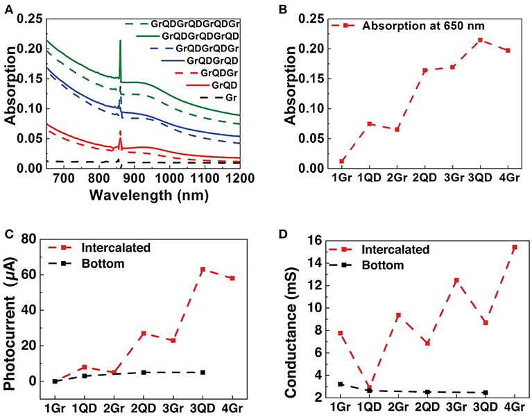
Figure 2. Light absorption, photocurrent (Iph) and conductivity evolution in Gr/QD films. (A) Light absorption of QDs films with intercalated graphene layers. The effect of adding graphene layers is minor compared with adding QD layers. (B) Light absorption (λ = 650 nm) evolution as Gr and QD layers are added, showing strong increment when QDs are added while Gr layers produce minor changes. (C) Evolution of Iph in intercalated devices show strong increments after adding QDs and minor reductions after adding Gr with an overall net increment as Gr and QDs are added. Bottom Gr device shows only a slight increase in Iph after adding QD layers. (D) Intercalated devices show increments in conductance after adding Gr layers with smaller but still significant reductions after adding QDs. As QDs and Gr layer are added there is a net increment in conductivity. Bottom Gr devices do not show significant changes as QDs are added. Photocurrent are measured under 532 nm laser diode, 0.9 mW.
A similar behavior can be observed in the evolution of the photocurrent (Iph = Ilight–Idark) for similar devices as shown in Figure 2C. The red line shows the evolution for intercalated devices, whereas the black line represents reference devices with a single bottom graphene layer but same number of QD layers as intercalated devices. Figure 2C shows that Iph has major increments only after adding QD layers as more photons are absorbed and photocarriers are generated. It can also be observed that Iph decreases slightly after Gr layers are added, but these setbacks are minor compared to the increments after adding QDs. For the non-intercalated devices (black line), Iphslightly increased from 3 to 5 μA as the thickness of QDs increased from 1QD layer (t~20 nm) to 3QD layers (t~60 nm). In contrast, for intercalated devices, Iph increased from 8 to 63 μA for 1QD layer (t ~20 nm) and 3QD layers (t ~60 nm).
The evolution in conductivity is shown in Figure 2D. The black line shows the conductivity of a device only with a Gr bottom layer, remaining fairly constant when adding more QDs. This is expected because QD films have poor conductivity. In contrast, for the intercalated device (red line), the conductance increases after Gr layers are added, improving the film conductivity for intercalated devices. However, after adding QDs, the conductivity is significantly reduced. This can be due to transfer of electrons from QDs to Gr, which would reduce charge carrier concentration on typical p-type Gr (Liu et al., 2011; Rath et al., 2011; Sun et al., 2012). The QDs can also affect the mobility and decrease the conductivity of Gr. Overall, the increase in conductivity by adding Gr layers is stronger than the negative effect of the QDs, as reflected on the overall increase in conductivity observed in Figure 2D. The conductance of the intercalated device with 3QDs (t = 60 nm) is 13.4 mS, whereas the bottom device with 3QDs stays low at 2.5 mS. Overall, the results in Figure 2 show that Gr has no major effect on light absorption of QD films, intercalated layers improve photocarrier collection, and adding Gr layers increase the overall conductivity of intercalated Gr/QD films.
Despite the improvements of intercalated films over bottom Gr devices, the short diffusion length, poor vertical conductivity, and the lack of vertical interconnects to Gr intercalated layers restrict the thickness of intercalated layers to ~200 nm (Chen et al., 2019). As shown in section Light penetration depth and transmission in QDs film, for λ = 850 nm, a QD film 200 nm thick can absorb only 20% of light radiation, wasting a significant amount of energy. Increasing the thickness to 400 nm would improve light absorption to 40% for such wavelength (section Light penetration depth and transmission in QDs film in Supporting Information). However, increasing the thickness would also reduce carrier collection. As the thickness increases, the photons absorbed in the top layers have a longer path to reach the bottom gold electrodes, reducing charge collection. To achieve thicker Gr/QD layers with efficient charge collection, we implemented two strategies: optimizing the distance between graphene layers (DGr in Figure 3A), and implementing gold contacts as VIAs to graphene layers (Figure 3B). Previous report on intercalated devices was based on one spin coating layer of QDs (DGr = 20 nm) in between graphene layers (Chen et al., 2019). However, it is known that QDs diffusion length (LD) is around 50–200 nm (Zhitomirsky et al., 2013; Lan et al., 2014, 2016; Stavrinadis et al., 2017). Intercalated devices with DGr = 20 nm, 60 and 100 nm were fabricated, all stacked 4 times, resulting in thicknesses of t = 80, 240, and 400 nm, respectively. The light ON/OFF response under λ = 532 nm illumination for these devices is shown in Figure 3C, showing the larger photoresponse for DGr = 60 nm. A plot of Iph vs. DGr for λ = 523 and 850 nm illumination as function of DGr (stacked 4 times, t = 4 × DGr) is shown in Figure 3E. The plots clearly show that the DGr = 60 nm (t = 240 nm) device gives the highest Iph. We infer that for DGr = 20 nm there is lower light absorption, reducing the photoresponsivity. For thicker devices with DGr = 100, 150, 200 nm (respective thickness of t = 400, 600, 800 nm) there is stronger light absorption, but the charge collection at the bottom gold contacts is poor, resulting in lower Iph. Graphene interspacing of DGr = 60 nm offers the best compromise between light absorption and carrier collection. Figure 3E also shows the compromise between charge collection and light absorption. For thinner films t < ~300 nm, the photoresponse for shorter wavelength (λ = 532 nm) is higher due to its shorter penetration depth and to the high collection efficiency of thin films. However, as the films become thicker, the photoresponsivity for short wavelengths drops drastically since the photons are mainly absorbed in the top layers and the photocarriers collection efficiency decays due to the longer path required to reach the bottom graphene layer. On the other hand, longer wavelengths (λ = 850 nm) have deeper penetration depth and its photogenerated carriers can reach the bottom graphene layer easier. Therefore, even though the photocurrent drops for both wavelengths, λ = 532 nm gives higher photoresponse for thin films and λ = 850 nm gives higher photoresponse for thicker films.
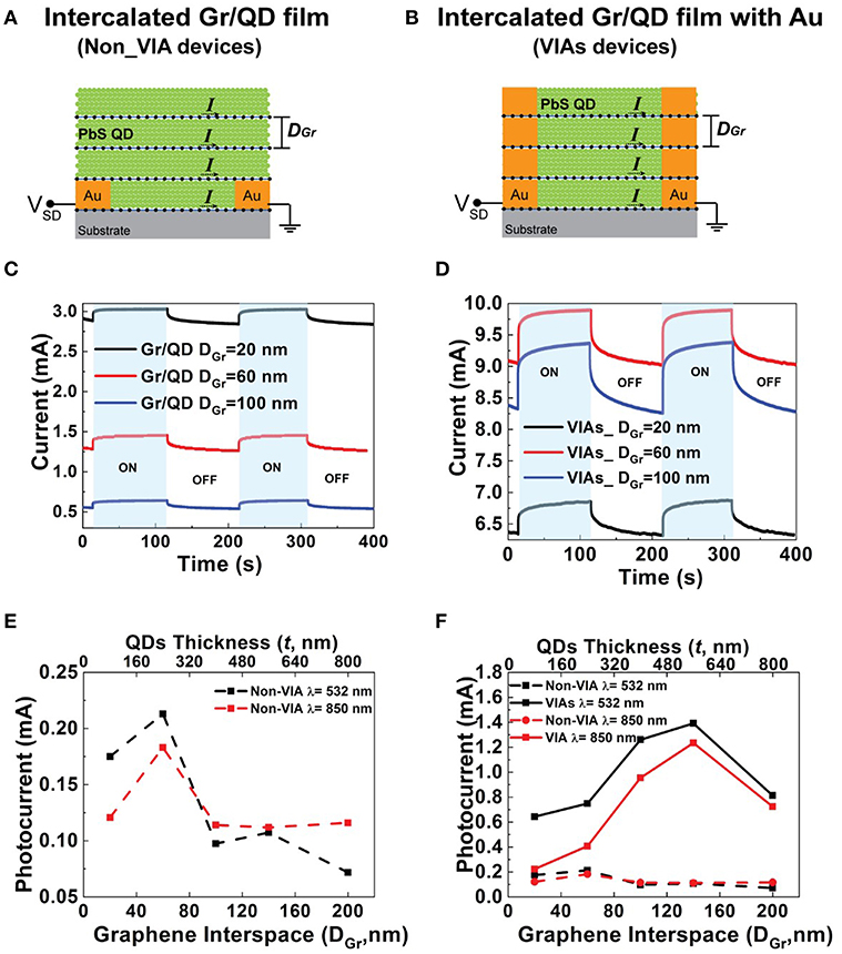
Figure 3. Graphene interspace (DGr) and Au VIAs. (A) Device configuration of intercalated Gr/QD devices showing the graphene interspacing parameter DGr without VIAs. (B) Device configuration with Au VIAs, connecting each Gr layer for enhanced charge collection. (C) Light ON/OFF response for non-VIAs devices as shown in (A) with DGr = 20, 60, 100 nm stacked 4 times with total thickness of t = 80, 240, and 400 nm, respectively. (λ = 532 nm, VDS = 1 V). (D) Light ON/OFF response for Au VIAs devices as shown in (B) with DGr = 20, 60, 100 nm stacked 4 times (t = 80, 240, and 400 nm, respectively). The response of VIAs devices is stronger than the corresponding non-VIAs devices in (C). (E) Iph vs. DGr (t = 4 × DGr) under λ = 532 and 850 nm light for non-VIAs devices, showing highest response with DGr = 60 nm. (F) Iph vs. DGr (t = 4 × DGr) under λ = 532 and 850 nm light for VIAs devices showing highest response with DGr = 140 nm. Measurements are under 532 nm (0.9 mW) and 850 nm (3.5 mW) laser diode illumination.
The most important improvement to overcome the poor vertical transport and reach thicker QDs film is the implementation of gold contacts that serve as VIAs to each Gr layer, as shown in Figure 3B. Charges collected at any Gr layer will be fully collected through the VIAs. The ON/OFF photoresponse for VIAs devices with DGr = 20 nm, 60 nm and 100 nm is shown in Figure 3D. Comparing VIAs devices in Figure 3D with non-VIAs devices in Figure 3C with same DGr and thickness shows that VIAs devices have a much higher Iph that we attribute to enhanced current collection through the gold interconnects. Figure 3F shows Iph vs. DGr (t = 4 × DGr) under λ = 532 and 850 nm illumination, both for VIAs and non-VIA devices, showing that VIAs devices have a stronger response for any DGr. In contrast to non-VIA devices, VIAs show a stronger Iph for DGr = 140 nm than for DGr = 60 nm, indicating the efficient collection through the Au contacts. It is also important to point that VIAs devices show increased response for both λ = 532 and λ = 850 nm (NIR) illumination. The VIAs structures therefore allow building thicker devices while keeping efficient charge collection.
The improved performance of VIAs over non-VIA devices over a range of light intensity is shown in Figure 4A. The increase in responsivity as function of light intensity has been reported for previous Gr/QD hybrid devices and is due to higher recombination rate, reduced built-in potential, and saturation of sensitizing traps in QDs as power increases (Yan et al., 2009; Konstantatos et al., 2012; Sun et al., 2012; Kufer et al., 2015). Despite the intercalated configuration, an electrostatic back gate is still capable of modulating carrier concentration in graphene layers. Figure 4B shows IDS vs. VG in light and dark conditions. In both cases, there is a clear signature of graphene, showing ambipolar conductivity, hitting a minimum when the Fermi level is at the Dirac point. In both cases the Dirac point is located at VG > 0 as well, indicating that the Fermi level is below the Dirac point in the valence band (p-doped). It is also clear that from dark to light there is a clear shift in the position of the Dirac point, shifting from VG = 65 V in dark to VG = 78 V under illumination, indicating a down shift in Fermi level, and therefore a transfer of holes from the QDs to Gr under illumination. The transfer of holes to p-doped results in increase conductivity. Figure 4C plots Iph vs. VG, demonstrating that the light response can be tuned with the back gate, allowing to even get a negative Iph for VG > 70 V.
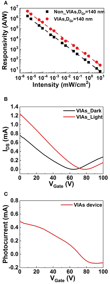
Figure 4. Light response dependence on intensity and gate voltage. Responsively increases as incident power decreases in log-log scale. VIAs device shows superior performance than non-VIA devices across different intensities. Linear plots are shown in section Photoresponse dependence on light intensity in Supporting Information. (B) IDS vs. VG in light and dark conditions for VIAs devices showing ambipolar graphene conductivity reaching the Dirac peak at VG = 65 V in dark and VG = 78 V in light. (C) Iph vs. VG for VIAs device, showing that photoresponse can be modulated through a gate voltage, reaching negative response for VG> 71.6 V. Gate current levels are under 70 nA both under dark and light conditions as shown in section IDS and IGate as a function of back-gate voltage in Supporting information. In all cases the device has DGr = 140 and t = 560 nm.
In conclusion, we have demonstrated the complementary role that Gr and QDs play in intercalated Gr/QD photodetectors and improved their performance by optimizing the graphene interspacing and adding gold contact VIAs on each graphene layer. The graphene layers have a minor impact on the light absorption of QD films and contribute to efficient charge collection of photocarriers produced by the QDs. The optimization of the graphene interspacing also allows for thicker films while keeping efficient charge collection. The intercalated Gr/QDs with VIAs show enhanced performance compared to conventional intercalated structure. The VIAs system helps to improve charge carrier collection and overcome the poor vertical conductivity, breaking the limitation of QDs film thickness in optoelectronic devices. This optimal intercalated Gr/QDs system with VIAs Au contacts can be the route to achieve thicker QDs film (t > 500 nm) enabling much stronger photoresponsivity and quantum efficiency for NIR light detection and showing potential for improved photovoltaic conversion using intercalated charge collectors.
Experimental Section
Device Fabrication
The hybrid photodetector used monolayer CVD graphene from Graphenea and PbS quantum dots from CANdots (Germany) with fluorescence at λem = 1,000 nm. Photolithography was used to define the electrode pattern on SiO2/Si (285 nm/500 μm) substrate. Chromium/gold (10/100 nm) was evaporated to form the electrodes with device dimension of 100 μm channel length and 800 μm channel width. Graphene was transferred onto the substrate by PMMA wet-transfer. PbS QDs films were deposited using spin-coating under ambient atmosphere. For each PbS QDs layer, the QDs solution (30 mg/mL in toluene) was spin-casted at 2,500 rpm for 30 s, then a solid-state ligand exchange was performed by flooding the surface with 0.03 M TBAI in methanol for 30 s before spinning dry at 2,500 rpm. For the bottom Gr/QD system, QDs film was formed layer-by-layer. The intercalated devices were realized by alternating graphene transfers with spin-coating of QDs films. For the VIAs devices, QDs were etched partially, then chromium/gold (10/100 nm) were deposited by e-beam evaporator, and Gr transfer QDs spin coating were carried out sequentially.
Photocurrent Measurements
Current-voltage data were measured with Keithley 2400 source meter, under dark and 532 nm (0.9 mW) and 850 nm (3.5 mW) laser diode illumination (CPS532-C2, CPS850 Thorlabs) in air.
Gate Measurement
Back gate was applied to the device as shown in IDS and IGate as a function of back-gate voltage in the Supplementary Material. Current were measured with Keithley 2400 source meter under dark and 532 nm (0.9 mW) laser diode.
Data Availability
The datasets generated for this study are available on request to the corresponding author.
Author Contributions
WC conceived the project. SA and CR implemented the back gate setup and performed the gate sweep measurements of the intercalated films. WC fabricated the devices and perform the photoresponsivity measurements. OV-M and WC wrote the manuscript. All the authors participated in the paper writing and analysis of the revised version.
Funding
This work was supported by the National Science Foundation under Award No. 1710472. This work was performed in part at the San Diego Nanotechnology Infrastructure (SDNI) of UCSD, NANO3, a member of the National Nanotechnology Coordinated Infrastructure, which is supported by the National Science Foundation (Grant ECCS-1542148).
Conflict of Interest Statement
The authors declare that the research was conducted in the absence of any commercial or financial relationships that could be construed as a potential conflict of interest.
Supplementary Material
The Supplementary Material for this article can be found online at: https://www.frontiersin.org/articles/10.3389/fmats.2019.00159/full#supplementary-material
References
Chen, W., Castro, J., Ahn, S., Li, X., and Vazquez-Mena, O. (2019). Improved charge extraction beyond diffusion length by layer-by-layer multistacking intercalation of graphene layers inside quantum dots films. Adv. Mater. 31:1807894. doi: 10.1002/adma.201807894
Clifford, J. P., Konstantatos, G., Johnston, K. W., Hoogland, S., Levina, L., and Sargent, E. H. (2009). Fast, sensitive and spectrally tuneable colloidal-quantum-dot photodetectors. Nat. Nanotechnol. 4, 40–44. doi: 10.1038/nnano.2008.313
He, R. X., Lin, P., Liu, Z. K., Zhu, H. W., Zhao, X. Z., Chan, H. L., et al. (2012). Solution-gated graphene field effect transistors integrated in microfluidic systems and used for flow velocity detection. Nano Lett. 12, 1404–1409. doi: 10.1021/nl2040805
Huo, N., and Konstantatos, G. (2018). Recent progress and future prospects of 2D-based photodetectors. Adv. Mater. 30, 1–27. doi: 10.1002/adma.201801164
Johnston, K. W., Pattantyus-Abraham, A. G., Clifford, J. P., Myrskog, S. H., Hoogland, S., Shukla, H., et al. (2008). Efficient Schottky-quantum-dot photovoltaics: the roles of depletion, drift, and diffusion. Appl. Phys. Lett. 92:122111. doi: 10.1063/1.2896295
Kagan, C. R., and Murray, C. B. (2015). Charge transport in strongly coupled quantum dot solids. Nat. Nanotechnol. 10, 1013–1026. doi: 10.1038/nnano.2015.247
Katsiev, K., Ip, A. H., Fischer, A., Tanabe, I., Zhang, X., Kirmani, A. R., et al. (2014). The complete in-gap electronic structure of colloidal quantum dot solids and its correlation with electronic transport and photovoltaic performance. Adv. Mater. 26, 937–942. doi: 10.1002/adma.201304166
Konstantatos, G., Badioli, M., Gaudreau, L., Osmond, J., Bernechea, M., Garcia de Arquer, F. P., et al. (2012). Hybrid graphene-quantum dot phototransistors with ultrahigh gain. Nat. Nanotechnol. 7, 363–368. doi: 10.1038/nnano.2012.60
Konstantatos, G., and Sargent, E. H. (2010). Nanostructured materials for photon detection. Nat. Nanotechnol. 5, 391–400. doi: 10.1038/nnano.2010.78
Koppens, F. H., Mueller, T., Avouris, P., Ferrari, A. C., Vitiello, M. S., and Polini, M. (2014). Photodetectors based on graphene, other two-dimensional materials and hybrid systems. Nat. Nanotechnol. 9, 780–793. doi: 10.1038/nnano.2014.215
Kufer, D., Nikitskiy, I., Lasanta, T., Navickaite, G., Koppens, F. H., and Konstantatos, G. (2015). Hybrid 2D-0D MoS2-PbS quantum dot photodetectors. Adv. Mater. 27, 176–180. doi: 10.1002/adma.201402471
Lan, X., Masala, S., and Sargent, E. H. (2014). Charge-extraction strategies for colloidal quantum dot photovoltaics. Nat. Mater. 13, 233–240. doi: 10.1038/nmat3816
Lan, X., Voznyy, O., García de Arquer, F. P., Liu, M., Xu, J., Proppe, A. H., et al. (2016). 10.6% certified colloidal quantum dot solar cells via solvent-polarity-engineered halide passivation. Nano Lett. 16, 4630–4634. doi: 10.1021/acs.nanolett.6b01957
Liu, Z., Li, J., Sun, Z. H., Tai, G., Lau, S. P., and Yan, F. (2011). The Application of highly doped single-layer graphene as the top electrodes of semitransparent organic solar cells. ACS Nano. 6, 810–818. doi: 10.1021/nn204675r
Mueller, T., Xia, F., and Avouris, P. (2010). Graphene photodetectors for high-speed optical communications. Nat. Photonics 4, 297–301. doi: 10.1038/nphoton.2010.40
Nikitskiy, I., Goossens, S., Kufer, D., Lasanta, T., Navickaite, G., Koppens, F. H., et al. (2016). Integrating an electrically active colloidal quantum dot photodiode with a graphene phototransistor. Nat. Commun. 7:11954. doi: 10.1038/ncomms11954
Rath, A. K., Bernechea, M., Martinez, L., and Konstantatos, G. (2011). Solution-processed heterojunction solar cells based on p-type PbS quantum dots and n-type Bi 2S 3 Nanocrystals. Adv. Mater. 23, 3712–3717. doi: 10.1002/adma.201101399
Saran, R., and Curry, R. J. (2016). Lead sulphide nanocrystal photodetector technologies. Nat. Photonics 10, 81–92. doi: 10.1038/nphoton.2015.280
Sargent, E. (2012). Colloidal quantum dot solar cells. Nat. Photonics 6, 133–135. doi: 10.1038/nphoton.2012.33
Stavrinadis, A., Pradhan, S., Papagiorgis, P., Itskos, G., and Konstantatos, G. (2017). Suppressing deep traps in PbS colloidal quantum dots via facile iodide substitutional doping for solar cells with efficiency >10%. ACS Energy Lett. 2, 739–744. doi: 10.1021/acsenergylett.7b00091
Sun, Z., Liu, Z., Li, J., Tai, G. A., Lau, S. P., and Yan, F. (2012). Infrared photodetectors based on CVD-grown graphene and PbS quantum dots with ultrahigh responsivity. Adv. Mater. 24, 5878–5883. doi: 10.1002/adma.201202220
Tang, J., and Sargent, E. H. (2011). Infrared colloidal quantum dots for photovoltaics: fundamentals and recent progress. Adv. Mater. 23, 12–29. doi: 10.1002/adma.201001491
van der Wiel, W. G., De Franceschi, S., Elzerman, J. M., Fujisawa, T., Tarucha, S., and Kouwenhoven, L. P. (2002). Electron transport through double quantum dots. Rev. Mod. Phys. 75, 1–22. doi: 10.1103/RevModPhys.75.1
Yan, F., Li, J., and Mok, S. M. (2009). Highly photosensitive thin film transistors based on a composite of poly(3-hexylthiophene) and titania nanoparticles. J. Appl. Phys. 106:074501. doi: 10.1063/1.3225760
Keywords: graphene, quantum dots, charge carrier collection, light absorption, optoelectronics
Citation: Chen W, Ahn S, Rangel C and Vazquez-Mena O (2019) Implementation of Metallic Vertical Interconnect Access in Hybrid Intercalated Graphene/Quantum Dot Photodetector for Improved Charge Collection. Front. Mater. 6:159. doi: 10.3389/fmats.2019.00159
Received: 12 May 2019; Accepted: 20 June 2019;
Published: 15 July 2019.
Edited by:
Peter Reiss, Commissariat à l'Energie Atomique et aux Energies Alternatives (CEA), FranceReviewed by:
Emmanuel Lhuillier, Institut des Nanosciences de Paris (INSP), FranceOleksandr Voznyy, University of Toronto Scarborough, Canada
Copyright © 2019 Chen, Ahn, Rangel and Vazquez-Mena. This is an open-access article distributed under the terms of the Creative Commons Attribution License (CC BY). The use, distribution or reproduction in other forums is permitted, provided the original author(s) and the copyright owner(s) are credited and that the original publication in this journal is cited, in accordance with accepted academic practice. No use, distribution or reproduction is permitted which does not comply with these terms.
*Correspondence: Oscar Vazquez-Mena, oscarvm@eng.ucsd.edu